
Method for producing photoelectric conversion device

a technology of photoelectric conversion and conversion device, which is applied in the field of photoelectric conversion device production, can solve the problems of large apparatus size, increased production cost, and uneven size and density of pinholes formed on the surface of the cigs layer, and achieves easy and evenly diffused multivalent cations, short time period, and increased diffusion density

Inactive Publication Date: 2013-09-19
FUJIFILM CORP
View PDF20 Cites 9 Cited by
  • Summary
  • Abstract
  • Description
  • Claims
  • Application Information

AI Technical Summary

Benefits of technology

The present invention provides a method for producing a photoelectric conversion device that can easily and evenly diffuse N-type dopant in a light absorption layer with a sufficient density of diffusion, and which can achieve a high photoelectric conversion efficiency. This method reduces the time required for forming a pn junction and allows for the use of a wider range of substrates, which suppresses production costs. Additionally, the use of a method for diffusing multivalent cations in a light absorption layer by electrodeposition by immersing at least the light absorption layer of a layered member composed of a lower electrode and the light absorption layer deposited on a substrate allows for overwhelmingly reducing the time required for forming a pn junction as compared to a general chemical bath deposition method using a high-concentration ammonia solution. These technical effects are desirable for the production of photoelectric conversion devices.

Problems solved by technology

Therefore, the sizes of the apparatuses are large, and there is a problem that a cost of production becomes higher.
Further, in the method disclosed in Patent Document 3, the size and the density of pinholes of the buffer layer (or the window layer) formed on the surface of the CIGS layer are not uniform.
Therefore, a pn junction may be extremely uneven, and there is a risk that electricity generation efficiencies vary.
Further, in general buffer layer formation, diffusion of n-type dopants is not sufficiently even, because they diffuse by entering Cu vacancies that are spontaneously generated on the surface of CIGS, or by substituting existing Cu.
Further, it is difficult to sufficiently increase the density of diffused n-type dopants while maintaining an appropriate thickness of the buffer.

Method used

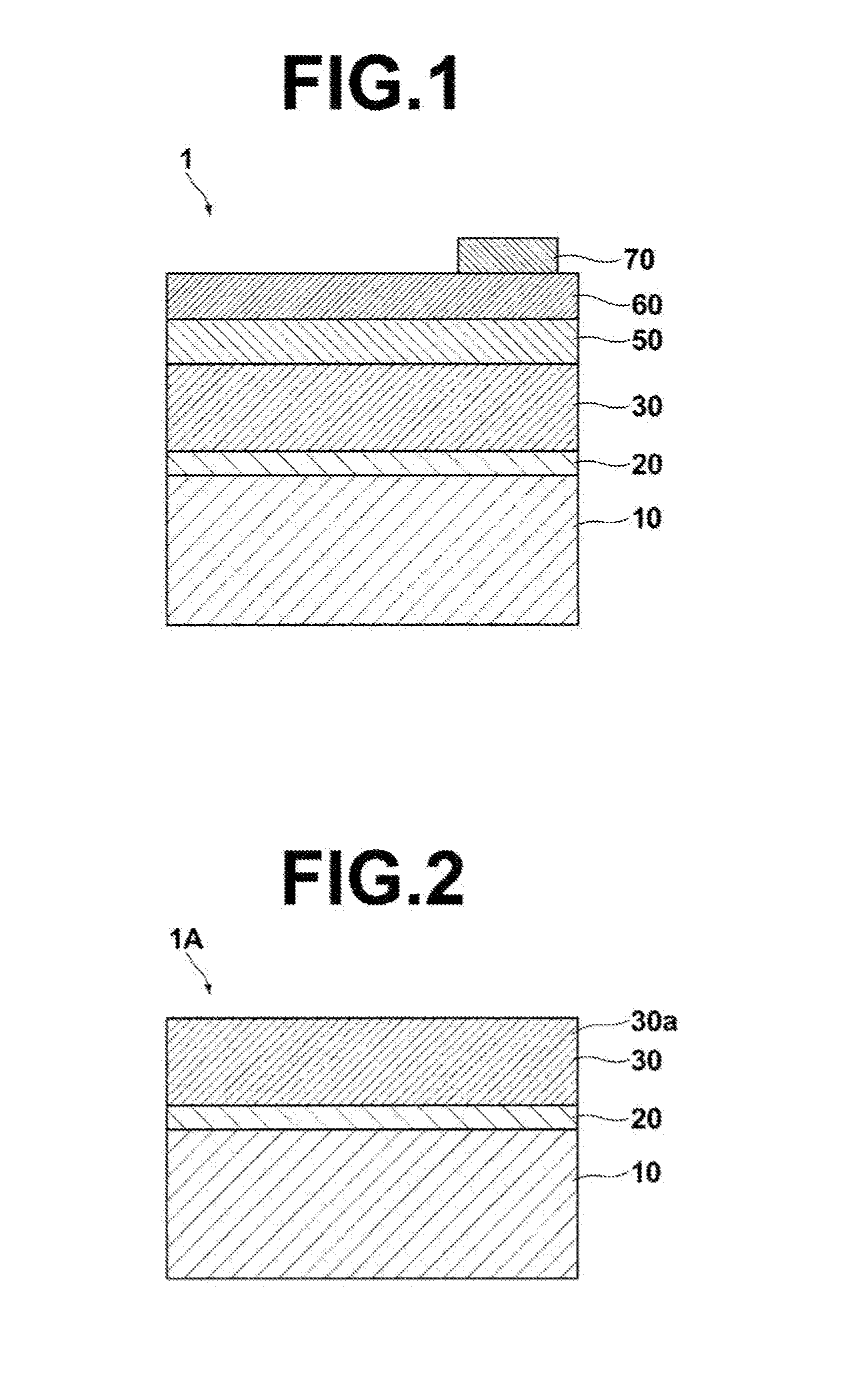
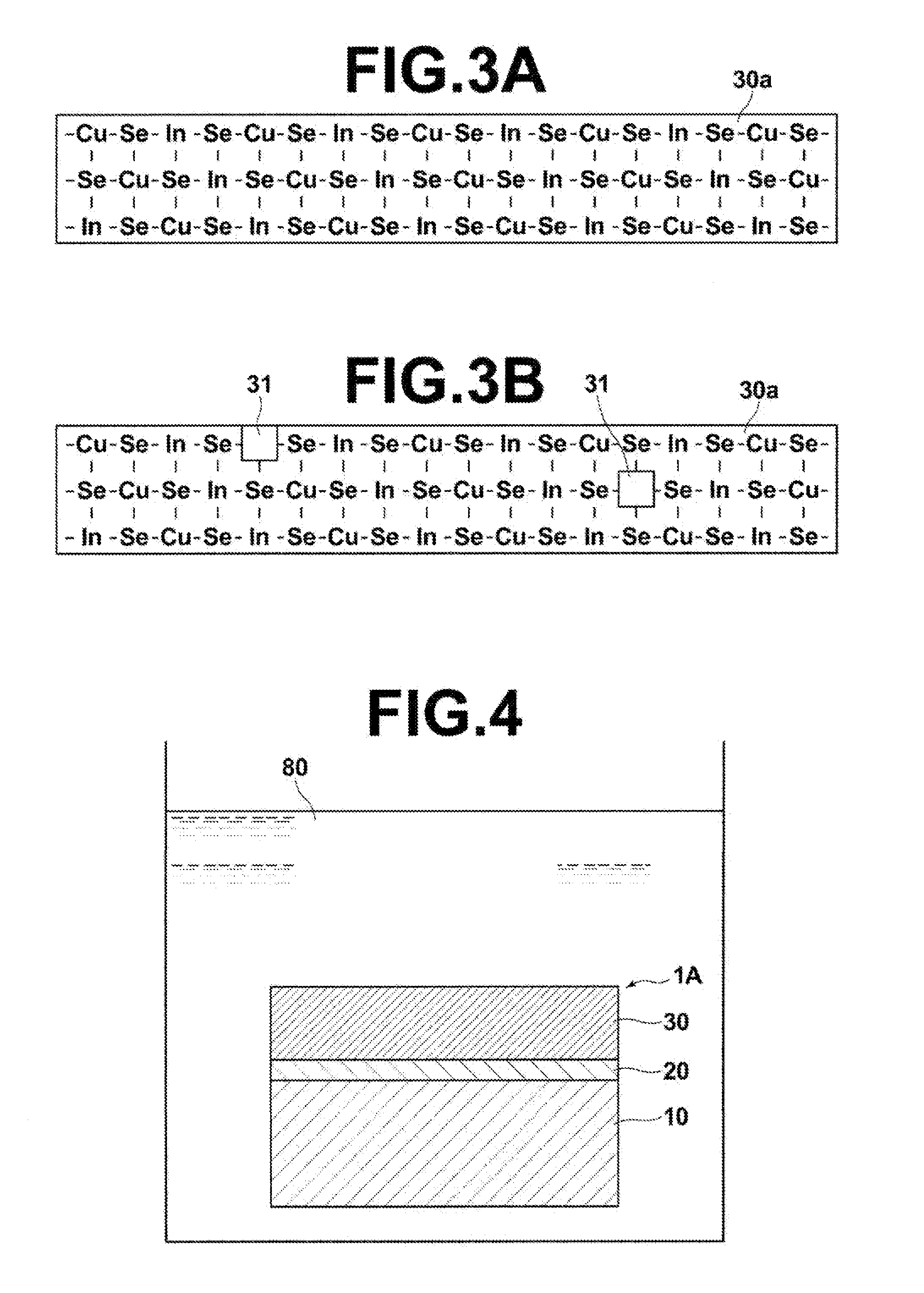

Image

  • Method for producing photoelectric conversion device
  • Method for producing photoelectric conversion device
  • Method for producing photoelectric conversion device

Examples


example 1-1

[0095]The layered member A was used.

Cu Vacancy Formation Process:

[0096]Tetraethylenepentamine (TEPA) was used as an amine species. A hydrogen peroxide solution of 1.35 weight % was mixed in an aqueous solution of TEPA of about 4.5 weight %. The layered member was immersed in the mixture for two minutes.

Pn Junction Formation Process:

[0097]The layered member after the vacancy formation process was immersed in an aqueous solution of zinc sulfate (pH 3.5). Further, voltage of 1.5 V was applied between a lower electrode and a counter electrode in such a manner that the electric potential on the lower electrode side was lower (the electric potential of the lower electrode was −1.5 V, and the electric potential of the counter electrode was 0 V). Accordingly, Zn2+, as multivalent cations, was diffused. The voltage was applied for five seconds.

example 1-2

[0098]The layered member A was used.

Cu Vacancy Formation Process:

[0099]Ethylenediamine was used as an amine species. A hydrogen peroxide solution of 1.35 weight % was mixed in an aqueous solution of ethylenediamine of about 3.2 weight %. The layered member was immersed in the mixture for two minutes.

Pn Junction Formation Process:

[0100]The process was performed under the same condition as Example 1-1.

example 1-3

[0101]The layered member A was used.

Cu Vacancy Formation Process:

[0102]Triethylenetetramine was used as an amine species. A hydrogen peroxide solution of 1.35 weight % was mixed in an aqueous solution of triethylenetetramine of about 3.6 weight %. The layered member was immersed in the mixture for two minutes.

Pn Junction Formation Process:

[0103]The process was performed under the same condition as Example 1-1.


PUM


Abstract

In a method for producing a photoelectric conversion device including a light absorption layer made of a CIGS-based compound semiconductor, a vacancy formation process for forming Cu vacancies in a surface layer of the light absorption layer in a layered member that is composed of a lower electrode and the light absorption layer deposited on a substrate is performed, and after then, a pn junction is formed in the surface layer of the light absorption layer.

Description

BACKGROUND OF THE INVENTION[0001]1. Field of the Invention[0002]The present invention relates to a method for producing photoelectric conversion devices used in solar cells, CCD sensors, or the like.[0003]2. Description of the Related Art[0004]A photoelectric conversion device including a photoelectric conversion layer (light absorption layer) and an electrode electrically connected to the photoelectric conversion layer is used for various purposes, such as solar cells. Conventionally, the main trend of solar cells was Si-based solar cells using bulk monocrystalline Si or polycrystalline Si, or a thin film of amorphous Si. However, research and development of compound semiconductor-based solar cells that do not rely on Si are being carried out. As the compound semiconductor-based solar cells, a bulk system, such as GaAs system, and a thin film system, such as CIGS system composed of a group Ib element, a group Mb element, and a group VIb element, are known. The CIGS-based semiconduc...

Claims


Application Information

Patent Timeline
Patent Type & Authority Applications(United States)
IPC IPC(8): H01L31/18
CPCH01L31/18H01L31/0322H01L31/0745H01L21/02664H01L21/02422H01L21/02491H01L21/02568Y02E10/541Y02P70/50
Inventor TADAKUMA, YOSHIO
Owner FUJIFILM CORP
Learn More