
Laminate with integrated electronic component

Inactive Publication Date: 2013-08-22
HERAEUS MATERIALS TECH
View PDF2 Cites 8 Cited by
  • Summary
  • Abstract
  • Description
  • Claims
  • Application Information

AI Technical Summary

Benefits of technology

The invention aims to improve the cooling and management of electronic components in laminates. It achieves this by connecting the electronic component directly to the second metal layer, which allows the component to dissipate its heat directly. The electronic component is connected through a thin layer of a connecting means, which is a good heat conductor. The invention reduces the number of thermal barriers, resulting in improved coupling of electronic components and stronger cooling. The laminate design has a low design height and allows for the utilization of the embossings and bulgings for reflecting radiation onto a sensor or emitting it from an LED. The invention simplifies the design and connection technology for the electronic component.

Problems solved by technology

This is disadvantageous in that the application of the conductive layer necessitates a second working step.
This is disadvantageous in that the inserted electronic component may overheat since the heat cannot be dissipated rapidly enough through the laminate.
This can impair the function, service life, and even the performance of the electronic component, even to the point of destruction thereof.
Another disadvantage is that an electronic component protrudes from the substrate after its conductor connectors are connected to the laminate.
Brittle chips might easily be destroyed.
It is also disadvantageous that the electronic component subsequently needs to be connected to the laminate.
This necessitates an additional working step that takes additional time in mass production and thus increases the production costs markedly.
Moreover, exact positioning of the electronic component may be difficult to achieve such that a certain fraction of inexactly positioned scrap is produced with the finished product and needs to be picked out subsequently.

Method used


Image

  • Laminate with integrated electronic component
  • Laminate with integrated electronic component
  • Laminate with integrated electronic component

Examples


Embodiment Construction

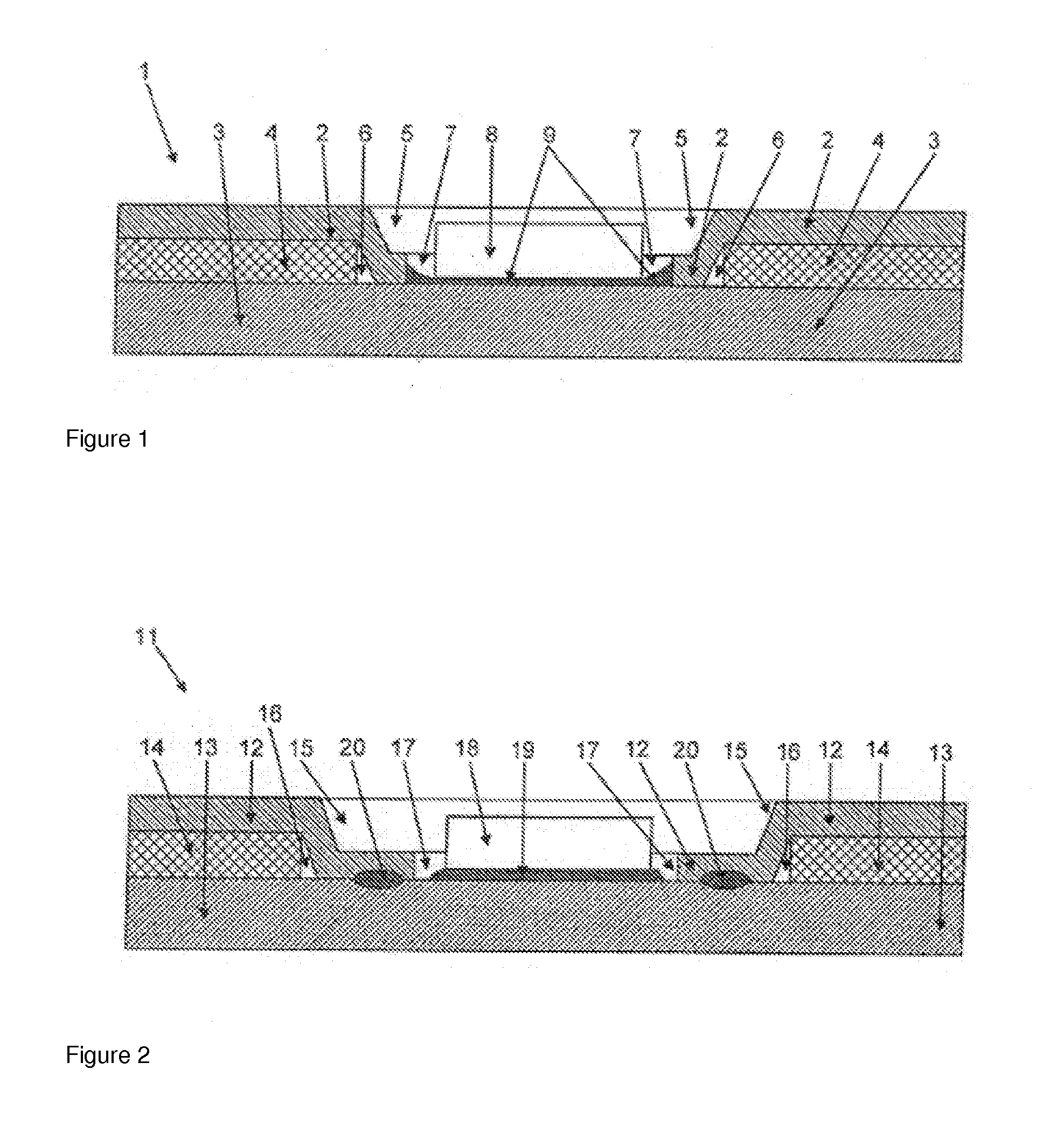
[0072]FIG. 1 shows a schematic cross-sectional view of a laminate 1 according to an embodiment of the invention or, as it may be, a schematic cross-sectional view of a laminate 1 produced using a method according to an embodiment of the invention. Laminate 1 comprises a first metal layer 2, a second metal layer 3, and an insulator 4 as insulating layer between the two metal layers 2, 3. The metal layers 2, 3 are applied to the insulator 4 by means of lamination technology.

[0073]An embossing 5 produced by means of embossing, deep-drawing or any other forming technique in a previously planar metal layer 2 is provided in the first metal layer 2. Alternatively, a bulging 5 can be provided that is produced during production of the first metal layer 2. Accordingly, a bulging 5 can also be produced alternatively by means of conferring a corresponding shape to the first metal layer 2 right away. For this purpose, the first metal layer 2 can be applied, for example, onto a corresponding moul...


PUM

PropertyMeasurementUnit
Heightaaaaaaaaaa
Surface areaaaaaaaaaaa

Abstract

The invention relates to methods for producing a laminate for contacting an electronic component, in which an insulating layer is arranged between first and second metal layers. The method includes contacting the metal layers to each other in a contact region, generating a recess in the insulating layer, laminating the metal layers to the insulating layer, generating a notch for accommodating the electronic component in the contact region in the first metal layer, inserting the electronic component in a depression in the laminate formed through a notch and recess. The electronic component is connected in a conductive manner to the second metal layer, such that an entire circumference of the electronic component is accommodated in the recess and / or notch, and at least part of the height of the electronic component is accommodated in the notch and / or recess. The invention also relates to such a laminate for contacting an electronic component.

Description

CROSS-REFERENCE TO RELATED APPLICATIONS[0001]This application is a Section 371 of International Application No. PCT / EP2011 / 005340, filed Oct. 24, 2011, which was published in the German language on May 10, 2012, under International Publication No. WO 2012 / 059187 A1 and the disclosure of which is incorporated herein by reference.BACKGROUND OF THE INVENTION[0002]The invention relates to a method for producing a laminate for contacting at least one electronic component, in which an insulating layer is arranged between a first metal layer and a second metal layer. The metal layers are contacted to each other in at least one contact region, at least one recess is or are generated in the insulating layer, and the metal layers are laminated to the insulating layer. The invention also relates to a laminate for contacting an electronic component. And lastly, the invention also relates to the use of the laminate.[0003]Integrated circuits (ICs, chips) are contacted in most cases by means of a ...

Claims


Application Information

Patent Timeline
IPC IPC(8): H05K1/02H05K3/10
CPCH01L23/13Y10T29/49155H01L23/498H01L33/60H05K1/0298H05K3/10H01L2224/48091H01L2224/48465H01L2224/73265H01L23/3735H01L2224/32013H01L2924/00014H01L2924/00
Inventor KLEIN, ANDREASDITZEL, ECKHARDKRUGER, FRANKKOCK, WULFHINRICH, ANDREAS
Owner HERAEUS MATERIALS TECH
Learn More