
Storage apparatus provided with a plurality of nonvolatile semiconductor storage media and storage control method

Active Publication Date: 2013-08-08
HITACHI LTD
View PDF16 Cites 43 Cited by
  • Summary
  • Abstract
  • Description
  • Claims
  • Application Information

AI Technical Summary

Benefits of technology

This patent describes a way to reduce the workload of a storage controller and ensure that data is evenly erased across different types of storage media. This results in a higher degree of accuracy and efficiency in the process.

Problems solved by technology

However, there is an upper limit to the frequency of write of data for the SSD and a length of life of an SSD is shorter than that of an HDD disadvantageously.
However, the number of times of a block erasing (hereafter referred to as a frequency of erasing) for each block is limited because of a physical restriction of a flash memory.
In other words, even in the case in which only a specific block can be suppressed from being degraded, an imbalance occurs to loads between SSDs and a load is concentrated solely on a specific SSD in some cases.

Method used


Image

  • Storage apparatus provided with a plurality of nonvolatile semiconductor storage media and storage control method
  • Storage apparatus provided with a plurality of nonvolatile semiconductor storage media and storage control method
  • Storage apparatus provided with a plurality of nonvolatile semiconductor storage media and storage control method

Examples


embodiment 1

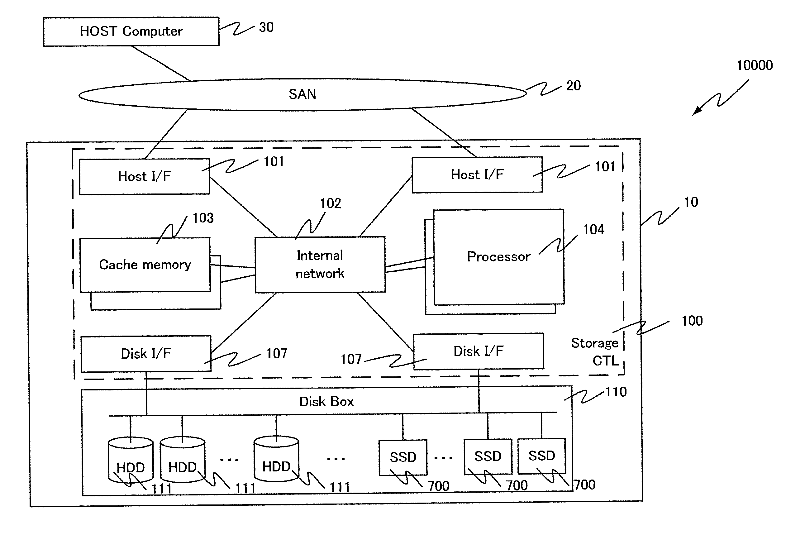
[0079]FIG. 1 is a view showing a configuration example of a storage system 10000 that includes a storage apparatus 10 in accordance with a first embodiment.

[0080]A storage system 10000 is provided with a storage apparatus 10 and a host computer 30.

[0081]The host computer 30 is an example of an upper level apparatus that utilizes the storage apparatus 10. The host computer 30 is an application server for instance. The host computer 30 and the storage apparatus 10 communicate with each other via a SAN (Storage Area Network) 20. As the SAN 20, a fiber channel, an SCSI (Small Computer System Interface), an iSCSI (internet Small Computer System Interface), a USB (Universal Serial Bus), an IEEE 1394 bus, and a SAS (Serial Attached SCSI) can be used for instance. As substitute for the SAN 20, a communication network of other type (such as a LAN (Local Area Network)) can also be adopted. In the figure, there is one host computer 30 and one storage apparatus 10. However, there can be a plura...

embodiment 2

[0342]An embodiment 2 will be described in the next place. The present embodiment includes many of common parts with the embodiment 1. Consequently, in the present embodiment, a part that is different from the embodiment 1 will be described mainly. In the case in which a WL target is selected in the embodiment 2, a predicted WA (see FIG. 36) is used in addition to the FM WR predicted amount.

[0343]Since a unique processing of the SSD such as a WL and a reclamation processing occurs in the SSD 700 in general, there is a characteristic in which an amount of data that is written to a flash memory as a practical matter is larger than an amount of data that has been received from the storage controller 100 by the SSD 700. This is called a WA (Write Amplification). An increase in a write data amount due to a processing in an SSD depends on an access pattern and a size of write data or the like.

[0344]In the case in which a write data amount is increased by a unique processing in the SSD, an...

embodiment 3

[0385]An embodiment 3 will be described in the next place. The present embodiment includes many of common parts with the embodiments 1 and 2. Consequently, in the present embodiment, a part that is different from the embodiments 1 and 2 will be described mainly.

[0386]In the embodiment 3, a granularity of the information that is acquired by the storage controller 100 is expanded in a Chunk unit. In this case, the statistics information 25200 shown in FIG. 17 can include the information 23210 in an SSD unit and the information 23220 in a Chunk (an aggregate of a plurality of extents) unit. Moreover, the address information 25100 (see FIG. 17) includes the information in a unit of an SSD and the logical physical conversion information in a Chunk unit.

[0387]Consequently, the processor 104 can comprehend a Chunk to which an extent belongs. In other words, the information that is acquired by the storage controller 100 for the present embodiment is more detailed as compared with that of th...


PUM


Abstract

A storage apparatus is provided with a plurality of nonvolatile semiconductor storage media and a storage controller that is a controller that is coupled to the plurality of semiconductor storage media. The storage controller identifies a first semiconductor storage unit that is at least one semiconductor storage media and a second semiconductor storage unit that is at least one semiconductor storage media and that is provided with a remaining length of life shorter than that of the first semiconductor storage unit based on the remaining life length information that has been acquired. The storage controller moreover identifies a first logical storage region for the first semiconductor storage unit and a second logical storage region that is provided with a write load higher than that of the first logical storage region for the second semiconductor storage unit based on the statistics information that indicates the statistics that is related to a write for every logical storage region. The storage controller reads data from the first logical storage region and the second logical storage region, and writes data that has been read from the first logical storage region to the second logical storage region and / or writes data that has been read from the second logical storage region to the first logical storage region.

Description

TECHNICAL FIELD[0001]The present invention relates to a storage control of a storage apparatus that is provided with a plurality of nonvolatile semiconductor storage media.BACKGROUND ART[0002]A storage apparatus is provided with a physical storage medium that is configured to store data and a controller that is configured to control a physical storage medium in general. The controller provides a data store space (a logical volume in general) to a computer (such as a host) that is coupled to a storage apparatus.[0003]A storage apparatus enables an I / O processing to be executed at a high speed and can show a high fault tolerance to a failure of a physical storage medium by using a plurality of physical storage media with a RAID (Redundant Array of Independent (or Inexpensive) Disks) configuration.[0004]A storage apparatus is equipped with an HDD (Hard Disk Drive) as a physical storage medium in general. In recent years however, a physical storage medium that is provided with a flash m...

Claims


Application Information

Patent Timeline
IPC IPC(8): G06F12/00
CPCG06F3/0616G06F3/0688G06F3/0647G06F3/0605G06F3/0608G06F3/0659G06F3/0665G06F3/067
Inventor KOSEKI, HIDEYUKIOGAWA, JUNJI
Owner HITACHI LTD
Learn More