Printed circuit board

Inactive Publication Date: 2013-07-04
CANON KK
View PDF5 Cites 4 Cited by
  • Summary
  • Abstract
  • Description
  • Claims
  • Application Information

AI Technical Summary

Benefits of technology

The present invention is about a printed circuit board that has a circuit element on it. The invention reduces the noise caused by the circuit element by stopping it from spreading.

Problems solved by technology

Printed circuit boards with a circuit element mounted thereon such as integrated circuit (IC) and large-scale integration (LSI) are known to have a problem: the circuit element in a printed circuit board causes electromagnetic wave noise when turned on / off, and the noise adversely affects the other circuits of the electronic device that incorporates the printed circuit board and the other electronic devices, leading to malfunction.
The noise is caused mainly by the parasitic capacitance component and the inductance component of the wiring structure electrically connecting circuit elements, and by the high-frequency current flowing through the electromagnetic coupling of these components.
In the operating frequency range exceeding hundreds of MHz, the parasitic components of a noise suppression element itself or the wiring structure in the printed circuit board more and more adversely affect the circuits, so that the noise suppression components cannot achieve their original function, providing only insufficient suppression effect.
However, in the embedded capacitor substrate using the entire power source conductor layer and ground conductor layer as electrodes, noise caused locally by operation of circuit element is propagated over the substrate, increasing radiation noise.

Method used


Image

  • Printed circuit board
  • Printed circuit board
  • Printed circuit board

Examples


examples

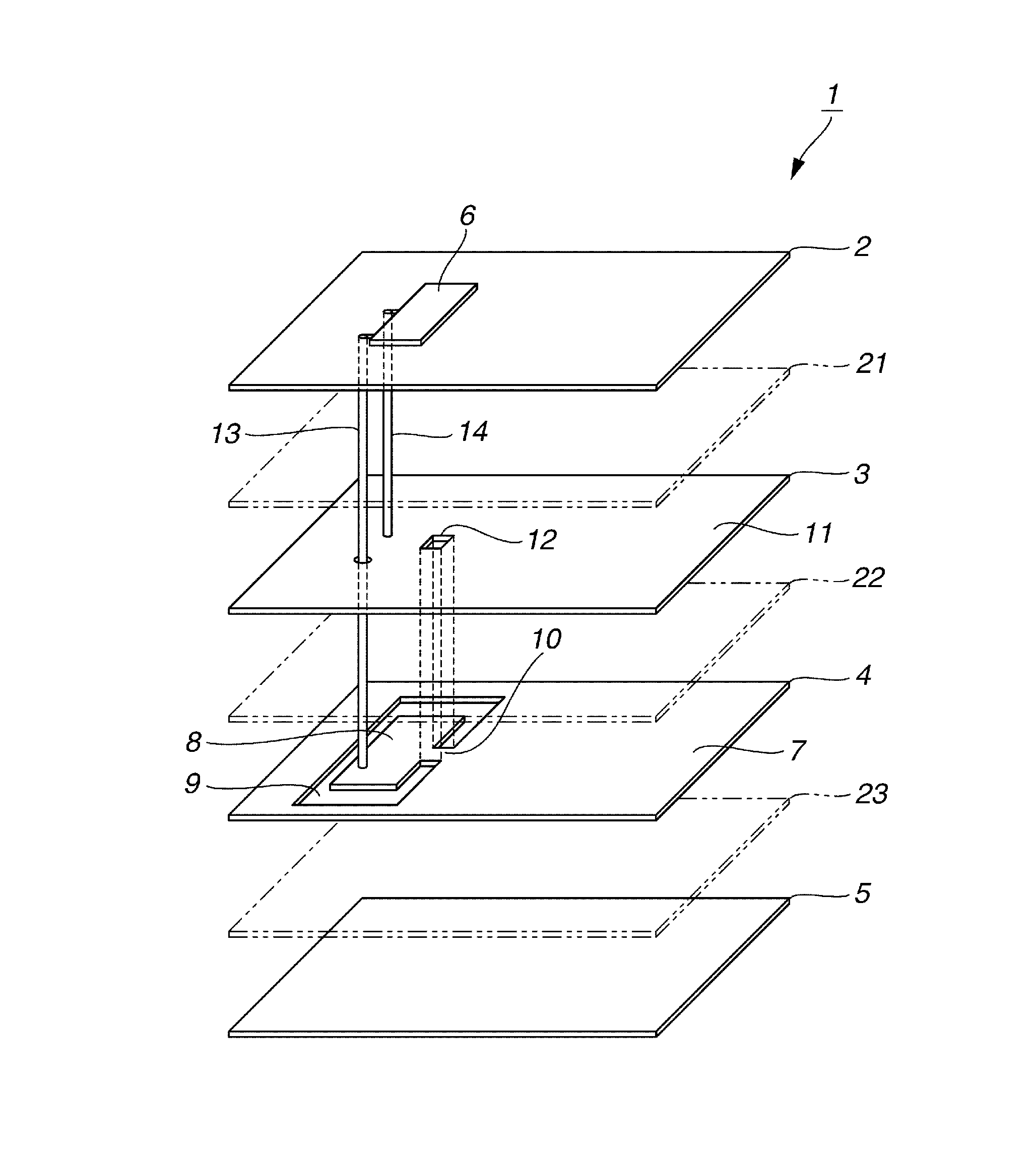
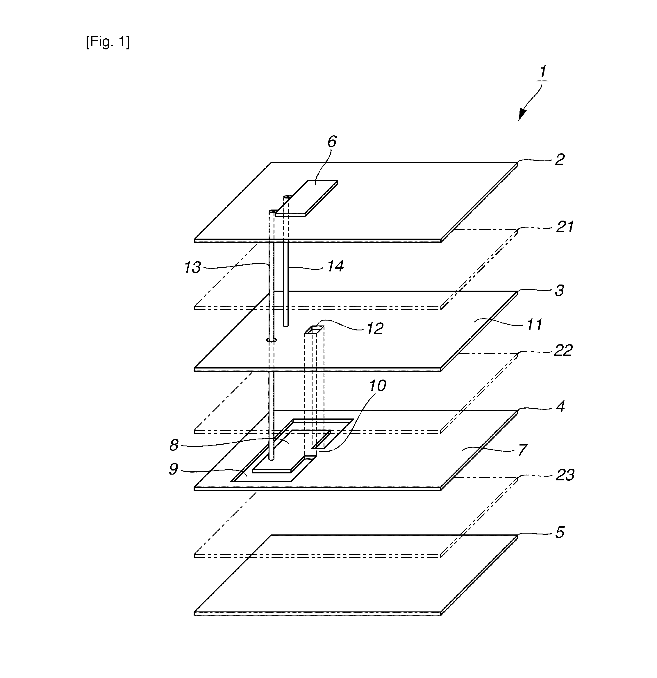
[0042]To verify the effect described in the above exemplary embodiment, a simulation was performed using an electromagnetic field simulation software, MW-Studio (manufactured by Computer Simulation Technology Inc. (CST)). FIG. 3 is an exploded perspective diagram illustrating wiring structures of conductor layers of a simulation model in the present Example. FIG. 3 illustrates the first signal wiring layer 2, the ground conductor layer 3, the power source conductor layer 4, and the second signal wiring layer 5. The printed circuit board 1 illustrated in FIG. 3 has a rectangular shape of 40 mm×90 mm. Each of the first signal wiring layer 2, the ground conductor layer 3, the power source conductor layer 4, and the second signal wiring layer 5 is made of a 50 micrometer thick copper.

[0043]Between the conductor layers, the insulator layers 21, 22, and 23 (see FIG. 1) each having a relative permittivity of 4.3 are interposed. The insulator layer 21 has a thickness of 100 micrometer, the ...


PUM


Abstract

A multi-layer printed circuit board includes an embedded capacitor substrate composed of a power source conductor layer and a ground conductor layer, the layers being disposed close to each other. The power source conductor layer has a first power source plane to supply power to a circuit element, and a second power source plane that is separated from the first power source plane by a gap and functions as a main power source. The first power source plane is partially connected to the second power source plane by a connecting line. The ground conductor layer has an opening at a position overlapping with a projected image when the connecting line is projected on the ground conductor layer. This structure suppresses propagation of the noise caused at the circuit element and reduces radiation noise in the printed circuit board.

Description

TECHNICAL FIELD[0001]The present invention relates to a printed circuit board having a circuit element thereon.BACKGROUND ART[0002]Printed circuit boards with a circuit element mounted thereon such as integrated circuit (IC) and large-scale integration (LSI) are known to have a problem: the circuit element in a printed circuit board causes electromagnetic wave noise when turned on / off, and the noise adversely affects the other circuits of the electronic device that incorporates the printed circuit board and the other electronic devices, leading to malfunction. The noise is caused mainly by the parasitic capacitance component and the inductance component of the wiring structure electrically connecting circuit elements, and by the high-frequency current flowing through the electromagnetic coupling of these components.[0003]In recent years, ICs and LSIs have extensively increased in processing speed to have operating frequencies from hundreds of MHz to several GHz. In the operating fre...

Claims


Application Information

Patent Timeline
IPC IPC(8): H05K1/02
CPCH01L23/49822H01L23/50H01L2924/0002H01L23/66H01L2223/6616H01L2924/1205H01L2924/14H05K1/0225H05K1/0233H05K1/0243H05K1/162H05K2201/093H05K2201/09345H05K2201/09663H05K1/0216H01L2924/00
Inventor MIYAZAKI, TOYOHIDEKOYAMA, KENJI
Owner CANON KK
Why Eureka
Try Eureka