
Negative electrode active material

a negative electrode active material and active material technology, applied in the manufacture of final products, cell components, conductors, etc., can solve the problems of increasing power consumption with multifunctionality, difficult to achieve a high charge/discharge capacity, and expansion of the volume of silicon (si) , to achieve excellent initial efficiency of a secondary battery and excellent cycle and efficiency properties

Active Publication Date: 2013-05-23
ILJIN ELECTRONICS
View PDF2 Cites 8 Cited by
  • Summary
  • Abstract
  • Description
  • Claims
  • Application Information

AI Technical Summary

Benefits of technology

The present invention relates to a negative electrode active material for a secondary battery. The material includes a phase A of active silicon and a phase B of a metal alloy matrix containing silicon and another transition metal. The material has a unique structure with a core of active silicon surrounded by a thin layer of metal alloy matrix. The metal alloy matrix has high hardness, excellent electric conductivity, and an electrochemical property. The material also has a fine structure that prevents expansion of the pole plate during charging and discharging, ensuring a long lifespan for the battery. The negative electrode active material of the present invention has excellent performance and can be used in secondary batteries.

Problems solved by technology

Portable electronic equipment is provided with a device having high power consumption, such as a central processing unit (CPU) and a liquid crystal display device (LCD), and shows increasing power consumption with multifunctionality.
As a widely used negative electrode active material, however, graphite has a problem in that it is difficult to achieve a high charge / discharge capacity.
However, a cell using silicon (Si) as a negative electrode material has a problem in that an expansion in volume of the silicon (Si) may take place during a charge cycle when lithium ions transferred to the negative electrode are intercalated into the silicon (Si).
Also, the lithium ions are deintercalated from the silicon (Si) during a discharge cycle, which leads to re-contraction of the silicon (Si).
In Japanese Patent Laid-open Publication No. 2006-286312, there have been attempts conducted to reduce the expansion and contraction of silicon (Si) using a physical shape of a silicon thin film, but the productivity of the thin film is severely lowered, which makes it difficult to apply the thin film to mass production of cells.

Method used


Image

  • Negative electrode active material
  • Negative electrode active material
  • Negative electrode active material

Examples


example 1

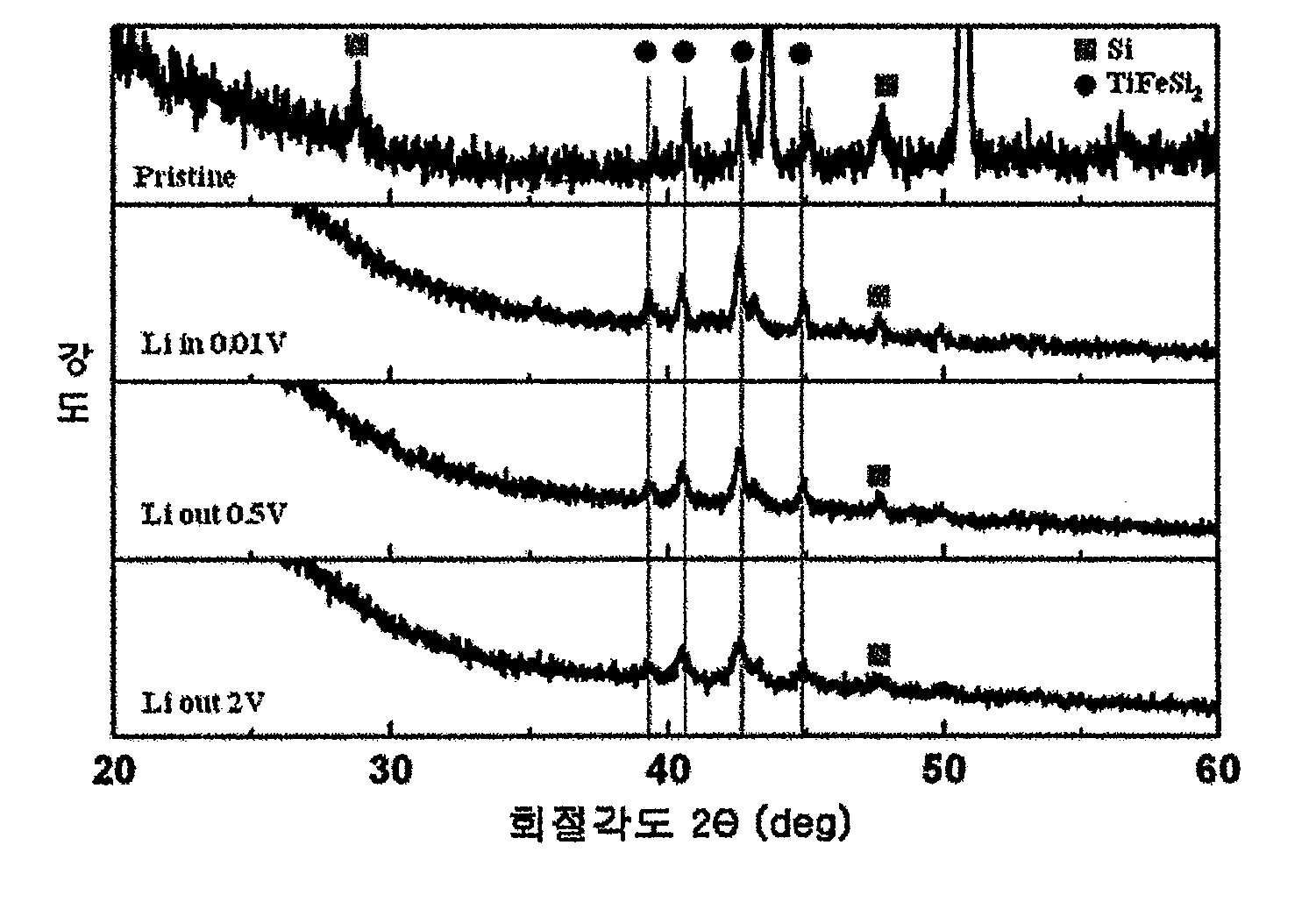
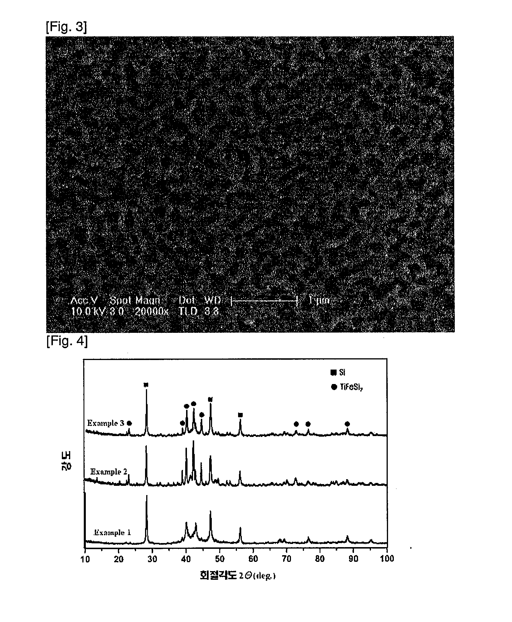
[0083]Silicon (Si), titanium (Ti) and iron (Fe) were mixed (Si:Ti:Fe=67%:16.5%:16.5%), and the resulting mixture was melted under argon gas using an arc melting method to prepare a Si—Ti—Fe crystalline alloy. The prepared alloy was subjected to a quenching method such as melt spinning, thereby preparing a negative electrode active material in which active silicon (Si) particles (phase A) were disposed in the Si—Ti—Fe alloy matrix (phase B) in a band shape. In the melt spinning method, the quenching rate (a rate of rotation of a kappa roll) was approximately 3,500 rpm.

example 2

[0084]A negative electrode active material was prepared in the same manner as in Example 1, except that the mixing ratio (Si:Ti:Fe) was altered to 70%:15%:15%.

example 3

[0085]A negative electrode active material was prepared in the same manner as in Example 1, except that the mixing ratio (Si:Ti:Fe) was altered to 74%:13%:13%.


PUM

PropertyMeasurementUnit
particle diameteraaaaaaaaaa
electric conductivityaaaaaaaaaa
thicknessaaaaaaaaaa

Abstract

A negative electrode active material and a secondary battery are provided. The negative electrode active material can be useful in maintaining excellent cell efficiency and lifespan while showing high-capacity properties, and the secondary battery may be manufactured using the negative electrode active material.

Description

CROSS-REFERENCE TO RELATED APPLICATION[0001]This application claims priority to and the benefit of Korean Patent Application No. 2010-0074314, filed Jul. 30, 2010, the disclosure of which is incorporated herein by reference in its entirety.BACKGROUND[0002]1. Field of the Invention[0003]The present invention relates to a negative electrode active material and a secondary battery.[0004]2. Discussion of Related Art[0005]A secondary battery is a chemical cell that can be repeatedly charged and discharged using an electrochemical reaction. One representative example of the secondary battery is a lithium secondary battery. In a lithium secondary battery, for example, a carbon-based material such as graphite is used for a negative electrode, a lithium-containing compound is used for a positive electrode, and a lithium salt is used for an electrolyte.[0006]Portable electronic equipment is provided with a device having high power consumption, such as a central processing unit (CPU) and a liq...

Claims


Application Information

Patent Timeline
Patent Type & Authority Applications(United States)
IPC IPC(8): H01M4/38
CPCH01M4/134H01M4/364H01M4/38H01M4/525H01M2004/021H01M10/0525H01M4/386Y02E60/122H01M4/581Y02E60/10Y02P70/50
Inventor KIM, JAE WOONGLEE, SEUNG CHULPARK, KI DUCKBAE, CHUL GYUKANG, JONG GOOCHO, YOON SEONG
Owner ILJIN ELECTRONICS
Learn More