Charge-domain filter and method thereof
- Summary
- Abstract
- Description
- Claims
- Application Information
AI Technical Summary
Benefits of technology
Problems solved by technology
Method used
Image
Examples
Embodiment Construction
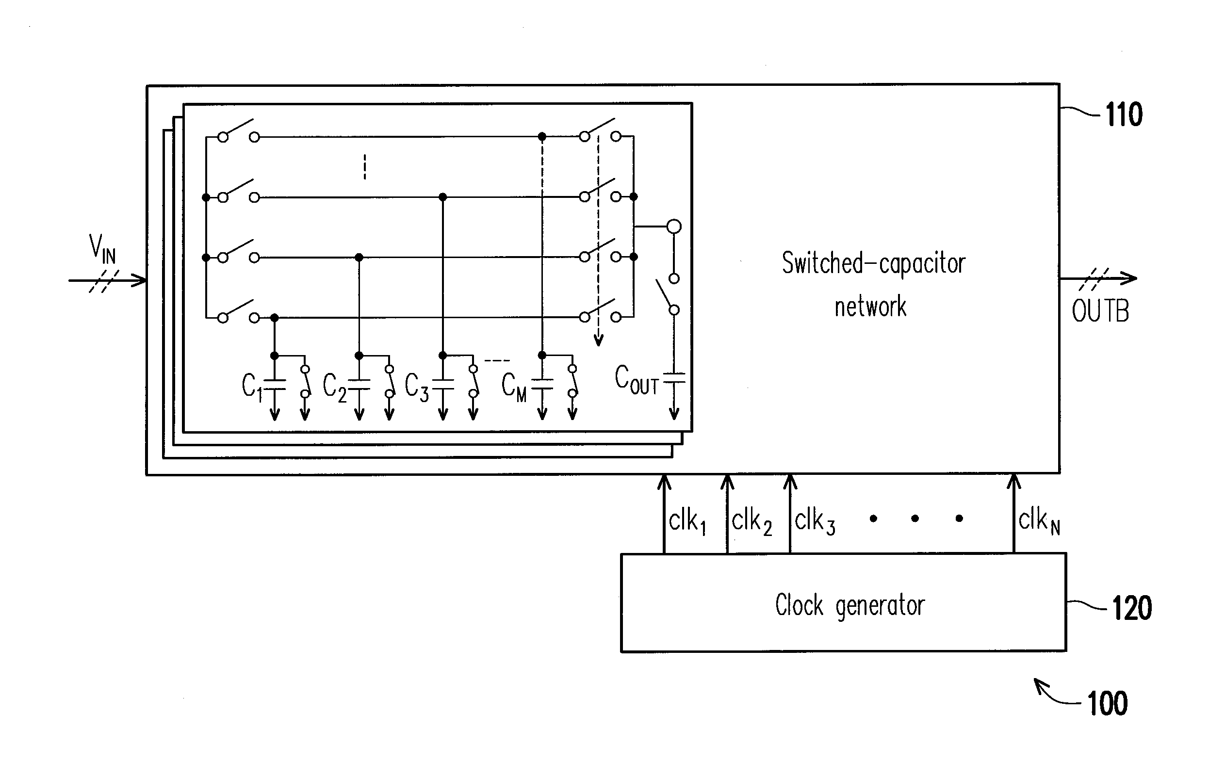
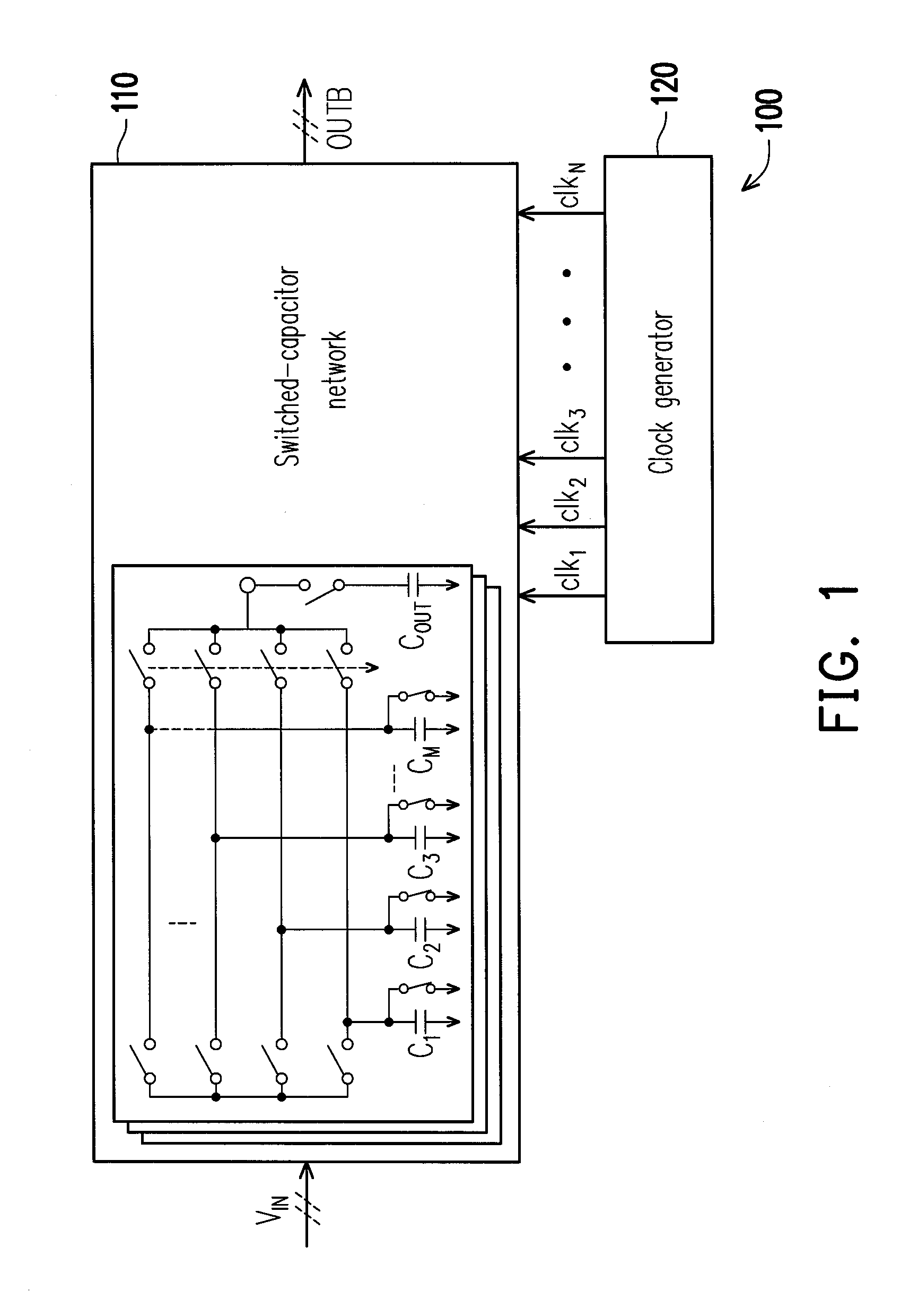
[0027]FIG. 1 is a functional block schematic diagram of a charge-domain filter (CDF) 100 according to an embodiment of the disclosure. The CDF 100 includes a switched-capacitor network (SCN) 110 and a clock generator 120. The clock generator 120 is coupled to the SCN 110 for providing N clock signals clk1, clk2, clk3, clkN. An input terminal of the SCN 110 receives an input signal V. The SCN 110 samples the input signal VIN according to the clock signals clk1-clkN, where the clock signals clk1-clkN have different phases. The SCN 110 filters the input signal VIN according to a discrete time signal processing method, and outputs a filtering result OUTB. Namely, by turning on / off a plurality of internal switches, the SCN 110 controls a charge storage status of internal capacitors, so as to perform the filter processing on the input signal VIN.
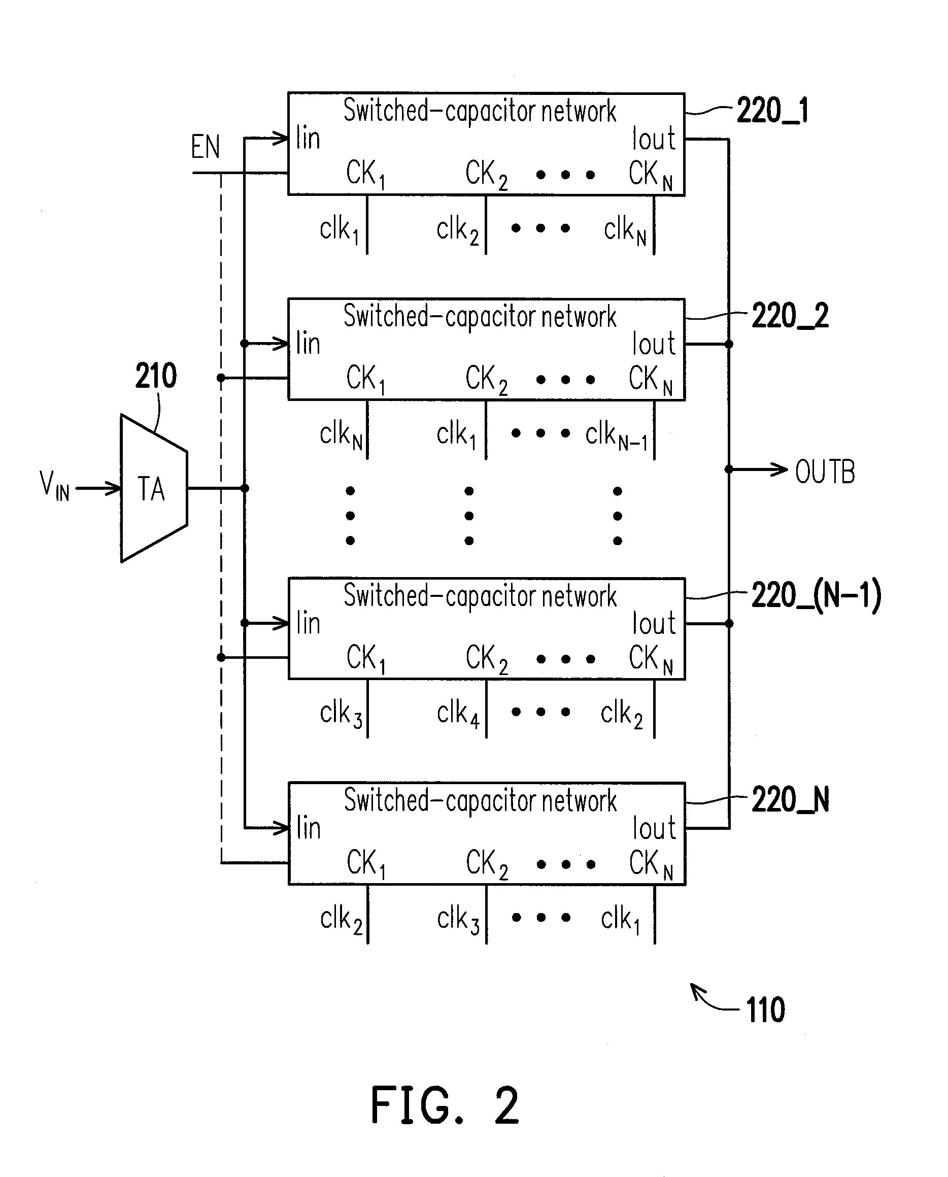
[0028]Any SCN or any CDF can be used to implement the aforementioned SCN 110. For example, FIG. 2 is a functional block schematic diagram of the ...
PUM
 Abstract
Description
Claims
Application Information
 - R&D Engineer
- R&D Manager
- IP Professional
- Industry Leading Data Capabilities
- Powerful AI technology
- Patent DNA Extraction
Browse by: Latest US Patents, China's latest patents, Technical Efficacy Thesaurus, Application Domain, Technology Topic, Popular Technical Reports.
© 2024 PatSnap. All rights reserved.Legal|Privacy policy|Modern Slavery Act Transparency Statement|Sitemap|About US| Contact US: help@patsnap.com


