Semiconductor device and operation method for same
a technology of semiconductor devices and mask sets, which is applied in semiconductor devices, digital storage, instruments, etc., can solve the problems of physical limit of devices, steep rise in the price of mask sets, and steep rise in the cost of lithography processes, and achieve low-voltage operation and high reliability.
- Summary
- Abstract
- Description
- Claims
- Application Information
AI Technical Summary
Benefits of technology
Problems solved by technology
Method used
Image
Examples
first exemplary embodiment
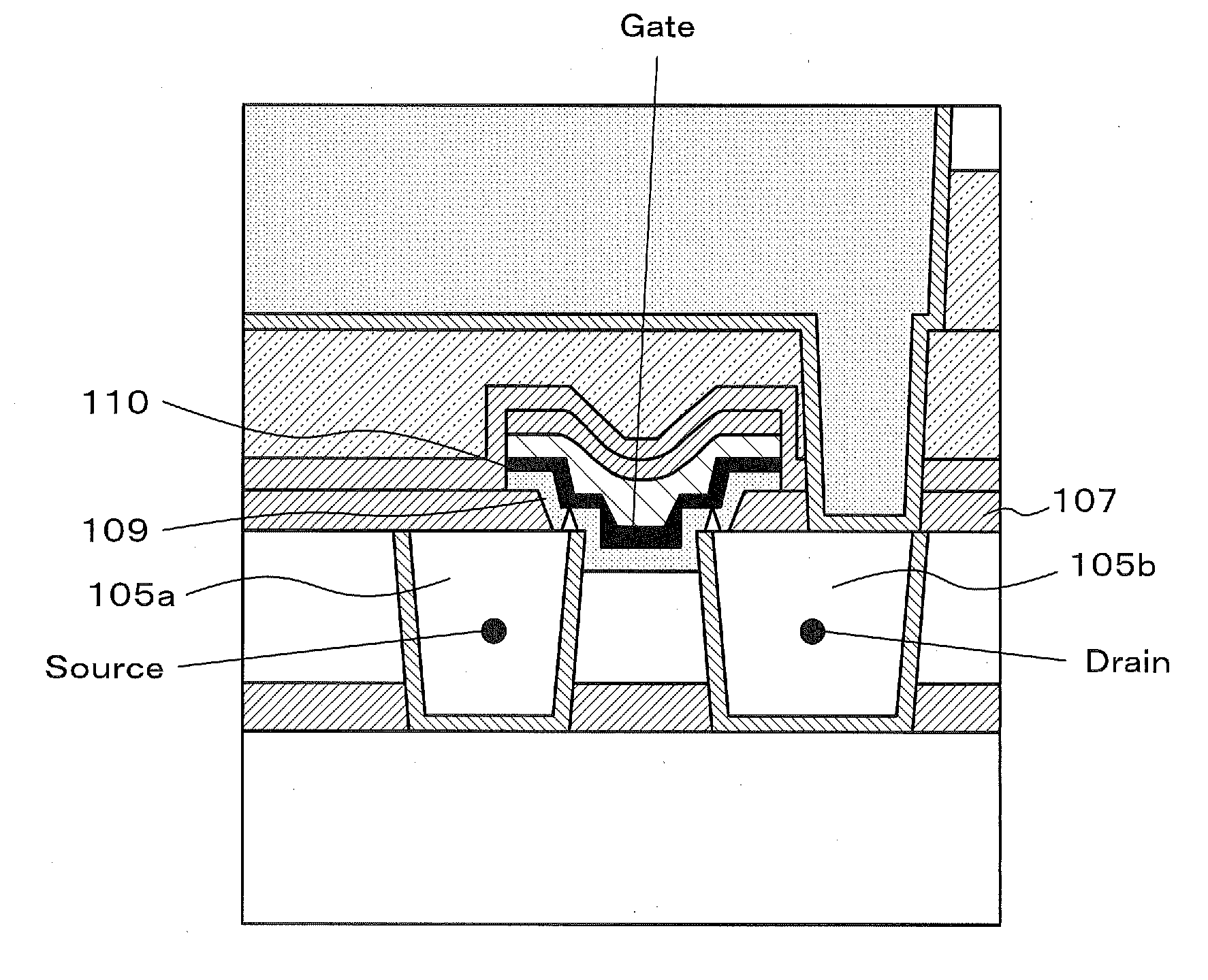
[0060]FIG. 3(A) is a schematic diagram showing the constitution of a semiconductor device according to a first exemplary embodiment. FIG. 3(B) shows a structure of the semiconductor device, while FIG. 3(A) shows a circuit diagram of the semiconductor device. The semiconductor device shown in FIG. 3 (A) includes a first switching element 1, a second switching element 2, and at least one third switching element 3. The third switching element 3 includes first and second terminals 31 and 32. Each of the first and the second switching elements 1, 2 includes ion conductors 13, 23, first electrodes 11, 21 which are disposed contacting with the ion conductors 13, 23 and supplies the metal ion to the ion conductors 13, 23, and second electrodes 12, 22 which are disposed contacting with the ion conductors 13, 23 and are less susceptible to ionization than the first electrodes 11, 21, respectively. The first electrode 11 of the first switching element 1 and the first electrode 21 of the second...
second exemplary embodiment
(Programming Method of Switching Element)
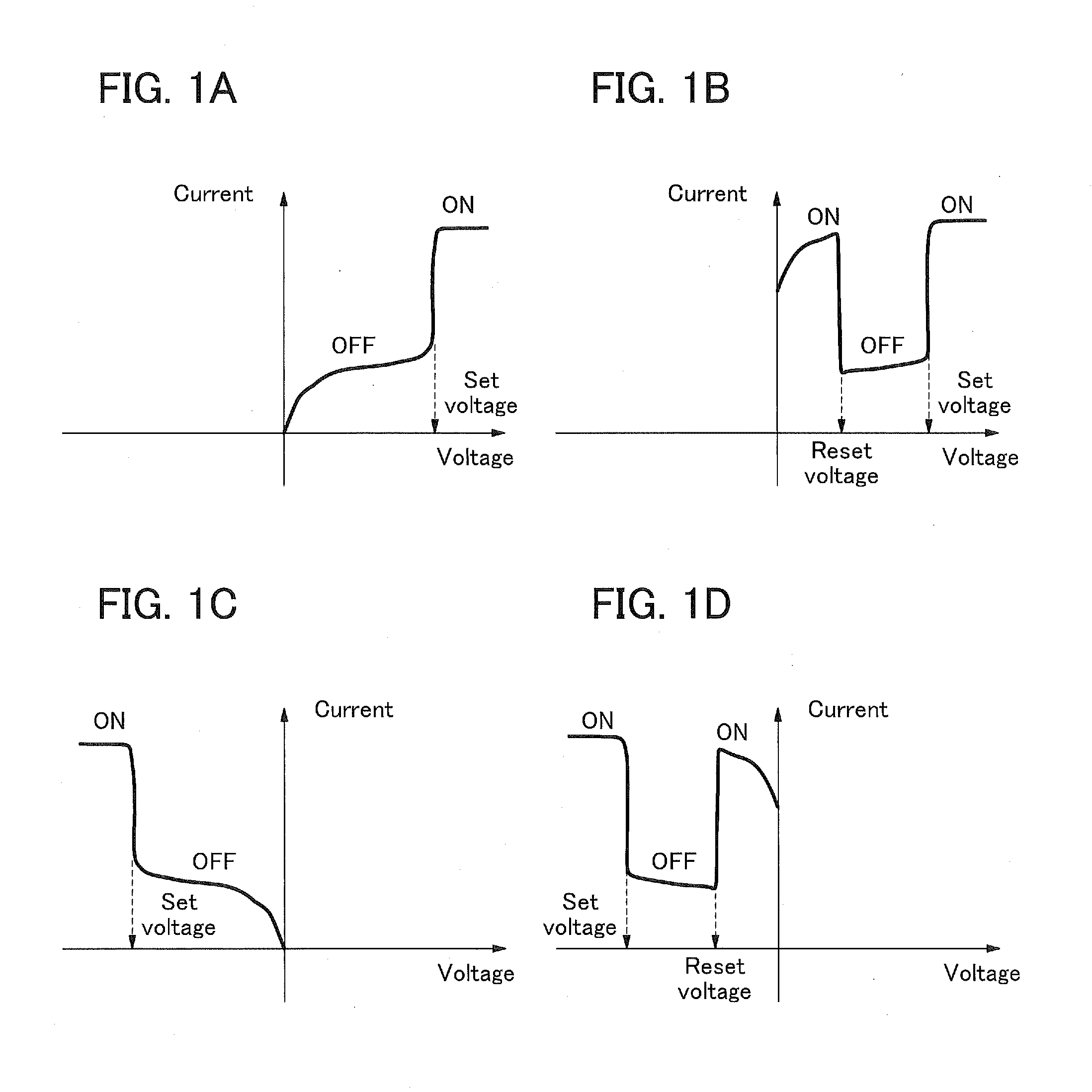
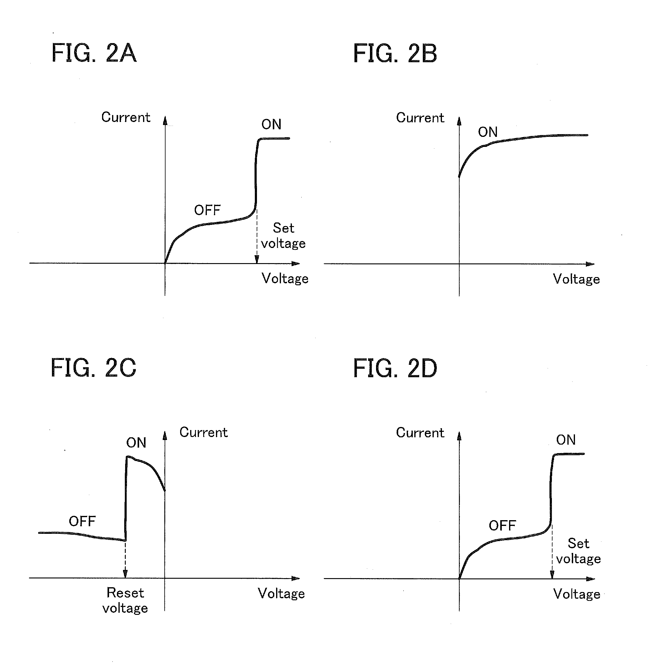
[0065]The method for programming the switching element according to the first exemplary embodiment will be described below. FIG. 6 is a schematic diagram showing a semiconductor device according to the second exemplary embodiment. As shown in FIG. 6, first electrodes of a first switching element 1 and a second switching element 2, and a drain of a first transistor 63 are electrically connected each other. Here, the first electrode 11 of the first switching element 1 and the first electrode 21 of the second switching element 2 are the active electrodes. A drain of a second transistor 61 is electrically connected to the second electrode 12 of the first switching element 1. Here, the second electrode 12 of the first switching element 1 is the inactive electrode. And a drain of a third transistor 65 is electrically connected to the second electrode 22 of the second switching element 2.
[0066]For example, if an electric signal is transmitted from a...
third exemplary embodiment
(Rewriting Circuit 1 Using P Type MIS and N Type MIS)
[0068]A semiconductor device according to a third exemplary embodiment is the same as the semiconductor device according to the second exemplary embodiment except that a programming method of the switching element is different from that of the second exemplary embodiment. FIG. 7 is a schematic diagram showing the semiconductor device according to the third exemplary embodiment. As shown in FIG. 7, a first electrode of a first switching element 1 and a first electrode of a second switching element 2, a drain of a first P type MIS (Metal Insulator Semiconductor) transistor 43 and a drain of a first N type MIS transistor 44, are electrically connected each other, respectively. Here, the first electrode 11 of the first switching element 1 and the first electrode 21 of the second switching element 2 are the active electrodes. A drain of a second P type MIS transistor 41 and a drain of a second N type MIS transistor 42 are electrically ...
PUM
 Abstract
Description
Claims
Application Information
 - R&D
- Intellectual Property
- Life Sciences
- Materials
- Tech Scout
- Unparalleled Data Quality
- Higher Quality Content
- 60% Fewer Hallucinations
Browse by: Latest US Patents, China's latest patents, Technical Efficacy Thesaurus, Application Domain, Technology Topic, Popular Technical Reports.
© 2025 PatSnap. All rights reserved.Legal|Privacy policy|Modern Slavery Act Transparency Statement|Sitemap|About US| Contact US: help@patsnap.com


