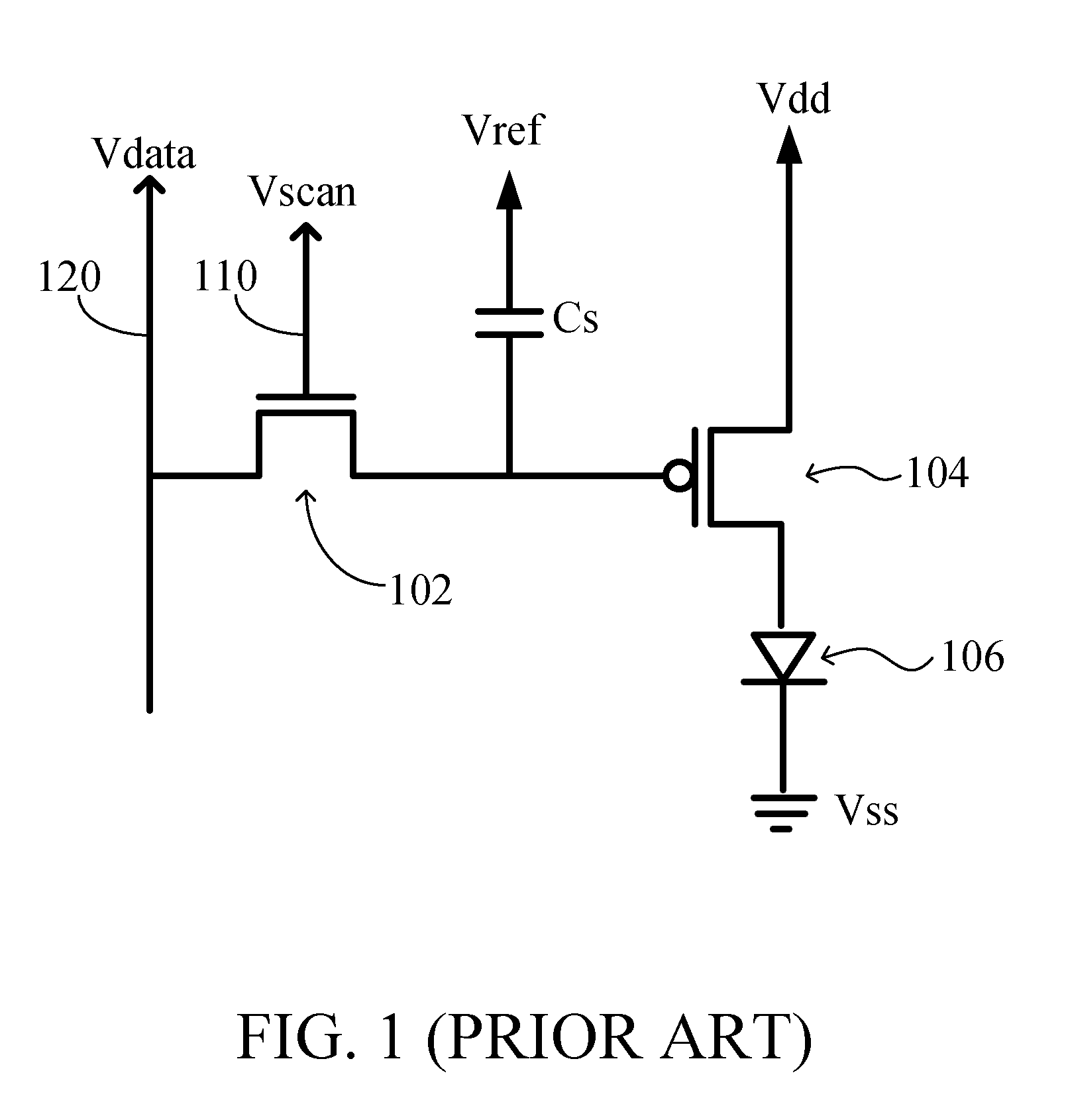
Pixel circuit and driving method thereof
a driving method and pixel technology, applied in the direction of lighting devices, instruments, light sources, etc., can solve the problems of non-uniformity of pixel current, inability to apply to high-definition displays, and inability to achieve uniform component characteristics, improve non-uniformity, and simplify the manufacturing process.
- Summary
- Abstract
- Description
- Claims
- Application Information
AI Technical Summary
Benefits of technology
Problems solved by technology
Method used
Image

Examples
Embodiment Construction
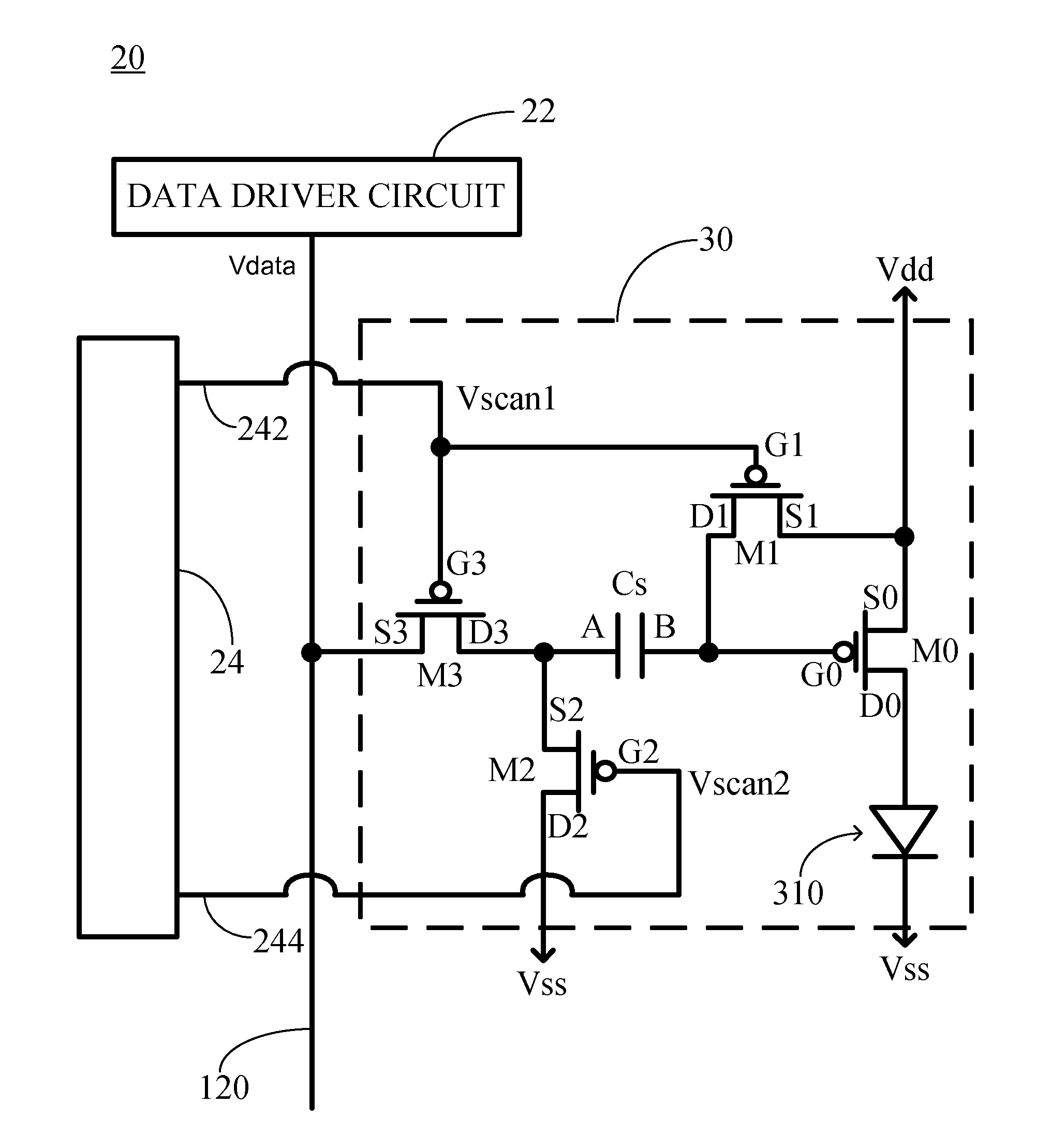
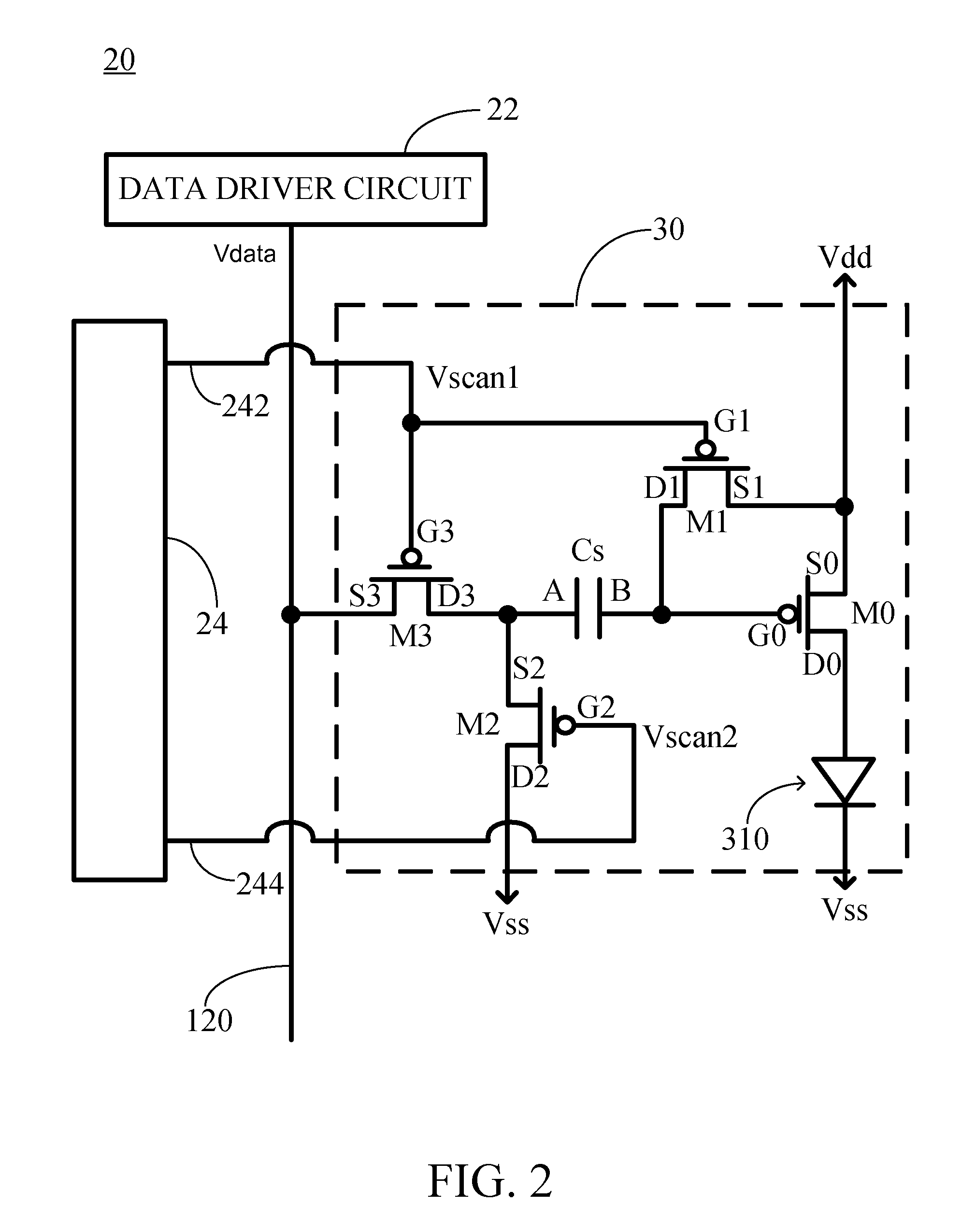
[0023]Referring to FIG. 2, FIG. 2 depicts a circuit diagram illustrating an AMOLED in one preferred embodiment of the present invention. The AMOLED 20 includes a data driver circuit 22, a scan driver circuit 24, and a plurality of pixel circuits 30, in which only a single pixel circuit 30 is depicted for clarity. The data driver circuit 22 provides a data signal Vdata via a data line 120, and the scan driver circuit 24 provides a first scanning signal Vscan1 and a second scanning signal Vscan2 respectively via a first scanning line 242 and a second scanning line 244.
[0024]In the embodiment, the pixel circuit 30 includes an LED 310, a storage capacitor Cs, a driving transistor M0, a first switching transistor M1, a second switching transistor M2, and a third switching transistor M3. Preferably, the LED 310 is an organic LED. Each of said transistors M0 to M3 has a control electrode, a first electrode and a second electrode. Preferably, each of the control electrodes is a gate G, and ...
PUM
 Abstract
Description
Claims
Application Information
 - R&D
- Intellectual Property
- Life Sciences
- Materials
- Tech Scout
- Unparalleled Data Quality
- Higher Quality Content
- 60% Fewer Hallucinations
Browse by: Latest US Patents, China's latest patents, Technical Efficacy Thesaurus, Application Domain, Technology Topic, Popular Technical Reports.
© 2025 PatSnap. All rights reserved.Legal|Privacy policy|Modern Slavery Act Transparency Statement|Sitemap|About US| Contact US: help@patsnap.com