
LED array capable of reducing uneven brightness distribution

a technology of led arrays and light emitting elements, which is applied in the direction of lighting and heating apparatus, instruments, transportation and packaging, etc., can solve the problems of uneven flow of electric current in the element, increased number of led elements is not preferable, and current decreases from the right power supply side to the left side, so as to reduce uneven brightness and reduce uneven brightness

Inactive Publication Date: 2013-02-28
STANLEY ELECTRIC CO LTD
View PDF1 Cites 10 Cited by
  • Summary
  • Abstract
  • Description
  • Claims
  • Application Information

AI Technical Summary

Benefits of technology

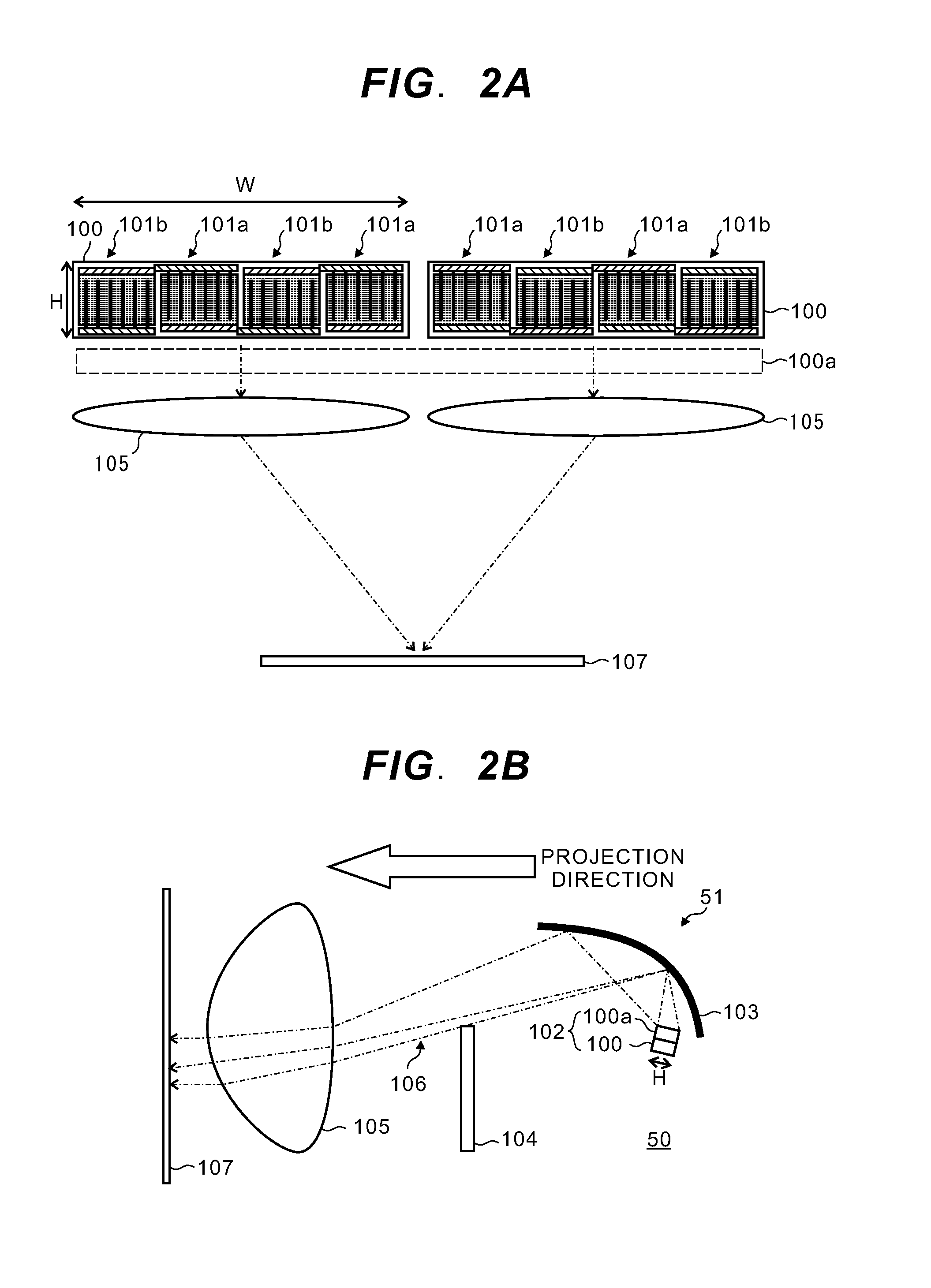
The present invention provides a semiconductor light emitting element array and an automotive lighting that can reduce uneven brightness distribution in a projection image. This means that the light emitting element array can create a more uniform brightness and the automotive lighting can produce a brighter and more consistent image.

Problems solved by technology

If a size of the element is simply enlarged, a driving electric current becomes too large and it becomes difficult to flow an electric current uniformly in the element.
However, increase in the number of LED elements is not preferable because a proportion of non-light-emitting regions between the elements increases.
Therefore, an injection current decreases from the right power supply side to the left side and it generates uneven brightness distribution.

Method used


Image

  • LED array capable of reducing uneven brightness distribution
  • LED array capable of reducing uneven brightness distribution
  • LED array capable of reducing uneven brightness distribution

Examples


Embodiment Construction

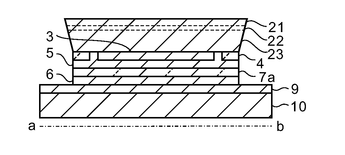
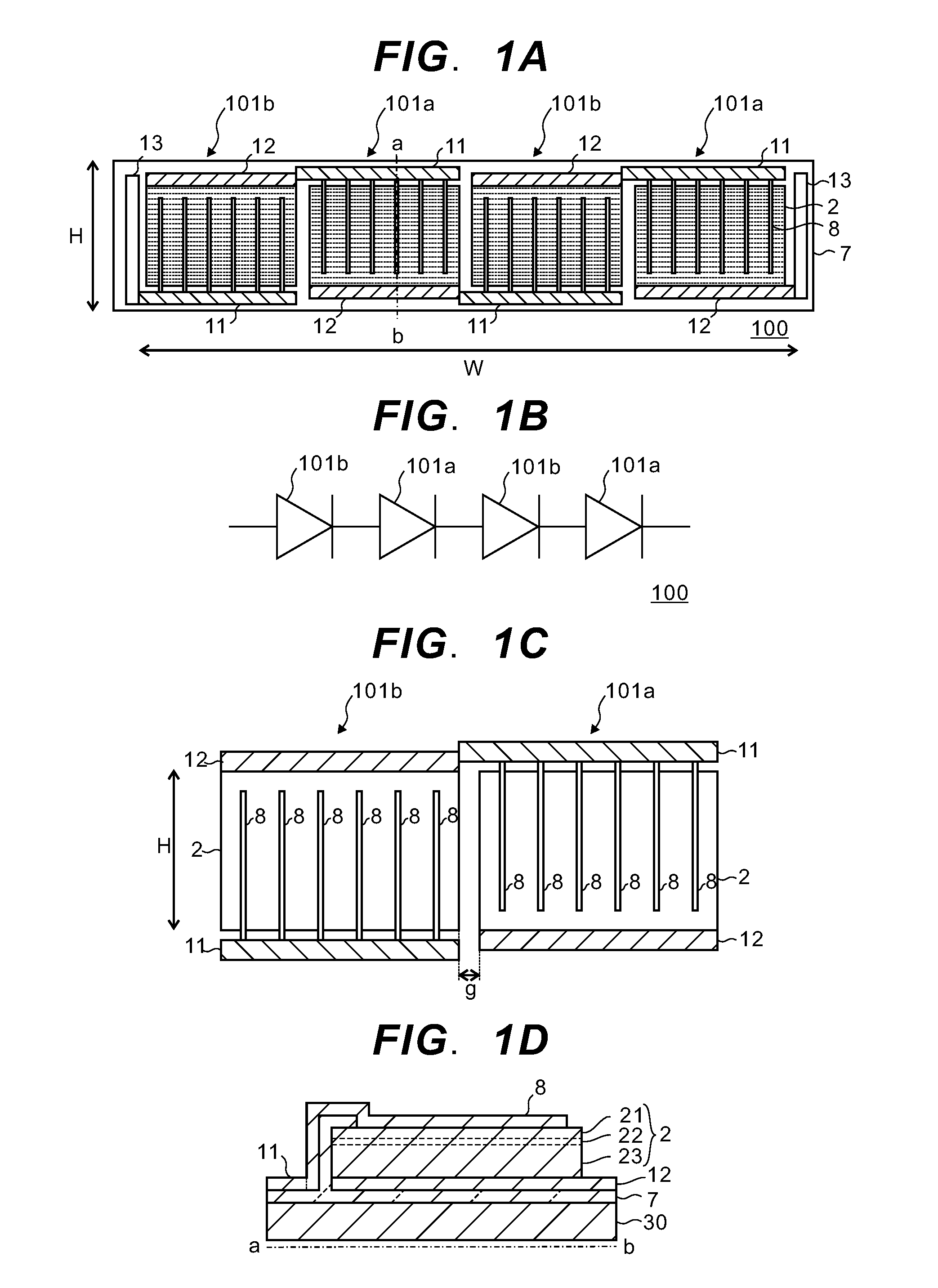
[0029]FIG. 1A is a schematic plan view of an LED array 100 according to a first embodiment of the present invention, and FIG. 1B is a circuit diagram of the LED array 100. FIG. 1C is a schematic plan view of LED elements 101a and 101b composing the LED array 100. FIG. 1D is a simplified cross sectional view of the LED array 100 cut along a line a-b in FIG. 1A. Moreover, hatching of the light emitting part 2 in FIG. 1A indicates brightness distribution wherein increase in density of hatching indicates increase in brightness.

[0030]The LED array 100 according to the first embodiment of the present invention is an array of four nitride semiconductor light emitting elements (LED elements) 101 (101a and 101b) connected in series and arranged along a W direction in the drawing on a supporting substrate 30 which is long in the W direction and on which an insulating layer 7 is formed. Each one of the LED elements 101 is an oblong which is long in the W direction and consists of a GaN-based l...


PUM


Abstract

A semiconductor light emitting array comprises a plurality of semiconductor light emitting elements disposed on an oblong substrate that is long in a first direction and arranged along with the first direction. Each light emitting element comprises an electrode layer formed on the substrate, a semiconductor light emitting layer formed on the electrode layer, stretched long in the first direction and comprising a p-type semiconductor layer, an active layer and an n-type semiconductor layer, a first wiring layer formed along and in parallel to one long side of the semiconductor light emitting layer, and second wiring layers extending to a direction of a short side from the first wiring layer and electrically connected to the n-type semiconductor layer on a surface of the semiconductor light emitting layer. The first wiring layers are disposed on different long sides of the semiconductor light emitting layers in the adjacent light emitting elements.

Description

CROSS-REFERENCE TO RELATED APPLICATION[0001]This application is based on Japanese Patent Application 2011-181449, filed on Aug. 23, 2011 and Japanese Patent Application 2011-191646, filed on Sep. 2, 2011, the entire contents of which are incorporated herein by reference.BACKGROUND OF THE INVENTION[0002]A) Field of the Invention[0003]This invention relates to a semiconductor light emitting element array and an automotive lighting using the semiconductor light emitting element arrays.[0004]B) Description of the Related Art[0005]High power is required for a light emitting diode (LED) element for use in headlamps for vehicles, illuminations or the likes. If a size of the element is simply enlarged, a driving electric current becomes too large and it becomes difficult to flow an electric current uniformly in the element. Therefore, in order to obtain a high power LED, a plurality of LED elements are arranged in a series to form an LED array (for example, refer to Japanese Laid-open Paten...

Claims


Application Information

Patent Timeline
Patent Type & Authority Applications(United States)
IPC IPC(8): G03B21/14H01L33/62
CPCH01L27/153H01L33/0079H01L33/38H01L33/385H01L33/62H01L2924/0002F21S48/1159H01L2924/00F21S41/147F21S41/151H01L33/0093H01L33/48
Inventor MIYACHI, MAMORUSAITO, TATSUMA
Owner STANLEY ELECTRIC CO LTD
Learn More