
Standard cells having transistors annotated for gate-length biasing

a technology of gate-length biasing and standard cells, applied in the direction of cad circuit design, program control, instruments, etc., can solve the problems of linear delay, exponential decrease of leakage power, and impairing time delay performance only linearly, so as to reduce leakage power and variability, reduce the impact of existing design and/or manufacturing processes, and add design space

Inactive Publication Date: 2013-01-10
RPX CORP
View PDF2 Cites 0 Cited by
  • Summary
  • Abstract
  • Description
  • Claims
  • Application Information

AI Technical Summary

Benefits of technology

The present invention provides a way to improve the performance of computer chips by making small changes to the length of the device gates in a way that doesn't impact existing processes. By biasing the gate lengths, leakage power can be reduced and delay can be minimized, resulting in improved performance and reduced power consumption. This technique can be used in various ways such as reducing power consumption, increasing signal integrity, improving manufacturability, and so on. The biasing can be applied to specific devices or to the entire chip layout.

Problems solved by technology

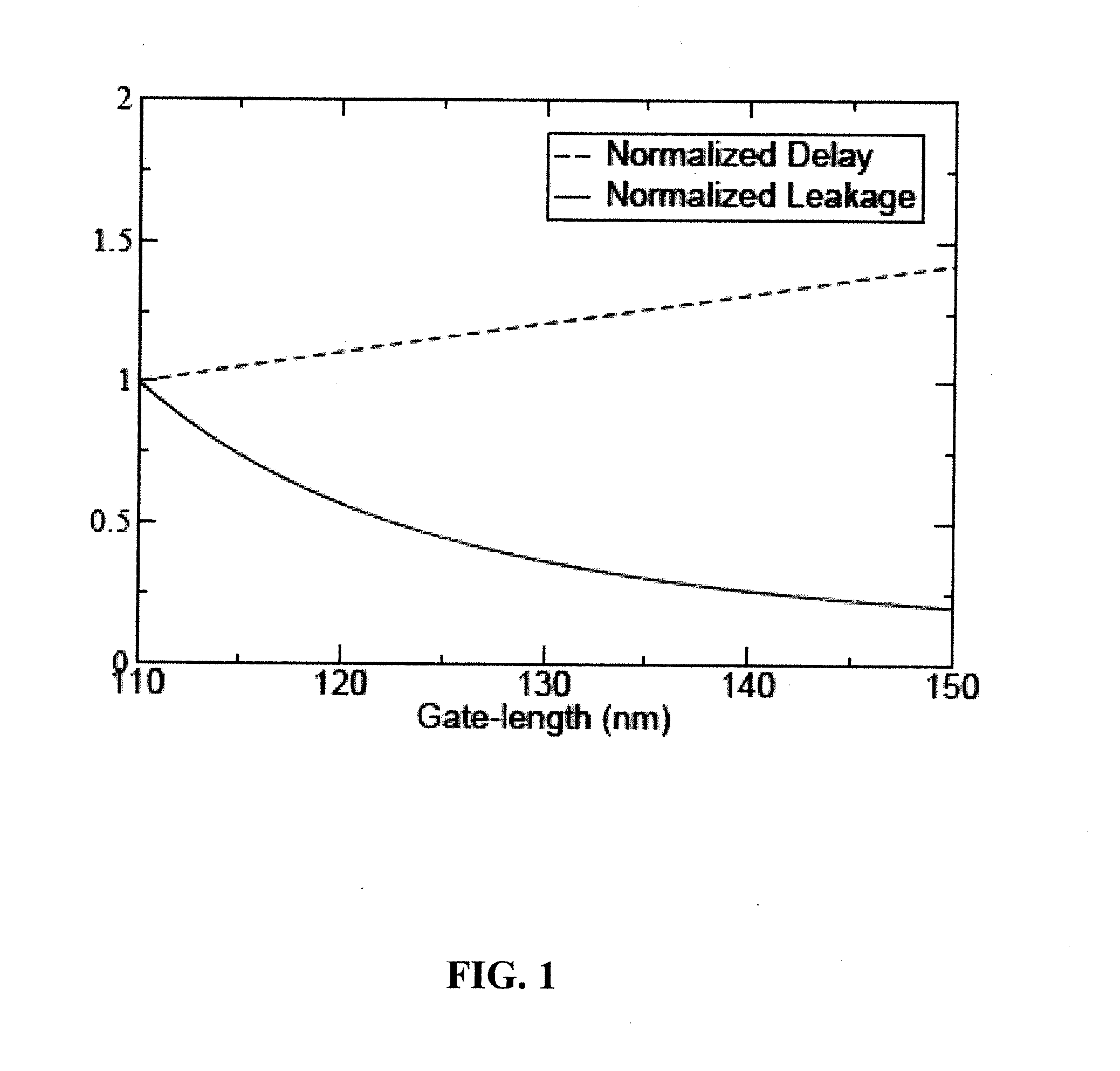
Typically, leakage power decreases exponentially, and delay increases linearly, with increasing gate-length.
Thus, it is possible to increase gate-length only marginally to take advantage of the exponential leakage reduction, while impairing time delay performance only linearly.

Method used


Image

  • Standard cells having transistors annotated for gate-length biasing
  • Standard cells having transistors annotated for gate-length biasing
  • Standard cells having transistors annotated for gate-length biasing

Examples


experimental examples

[0080]A test flow for validation of the LGate biasing methodology was implemented in the context of leakage reduction. Seven test cases were chosen for investigation. Details of the test cases used in the experiments are given in Table 3. For each test case, Table 3 shows the source of the test case, the number of cells in the circuit, delay, leakage power, and dynamic power. Sequential test cases (e.g., those beginning with “s”) were handled by converting them to combinational circuits by treating all flip-flops as primary inputs and primary outputs. The test flow was designed to validate an LGate biasing methodology in which CLLB was performed first followed by TLLB to show further reductions in leakage. Thus, while library generation and design optimization are discussed primarily with respect to the CLLB method, the discussion applies as well to the TLLB method.

TABLE 3TestLeakageDynamicCaseSource#CellsDelay (ns)(mW)(mW)s9234ISCAS′898610.4370.70740.3907c5315ISCAS′8514420.5561.441...


PUM


Abstract

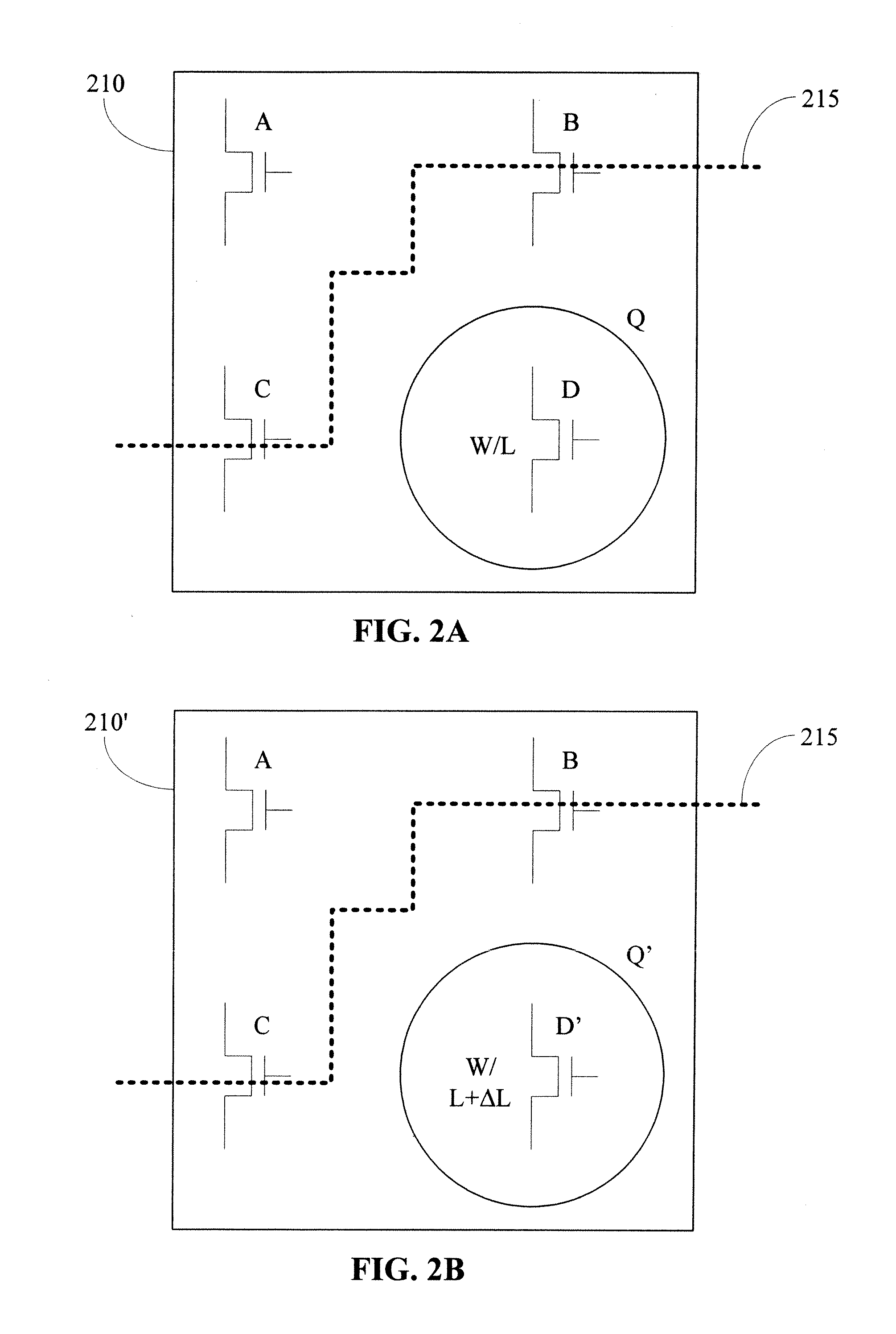
A standard cell library is disclosed. The standard cell library contains cells wherein at least one transistor in at least one cell is annotated for gate length biasing. Gate length biasing includes the modification of the gate length, so as to change the speed or power consumption of the modified gate length. The standard cell library is one used in the manufacturing of semiconductor devices (e.g., that result as semiconductor chips), by way of fabricating features defined on one or more layouts of geometric shapes. The annotations serve to identify which ones of the transistor gate features are to be modified before using the geometric shapes for manufacturing the semiconductor device.

Description

CLAIM OF PRIORITY[0001]This application is a continuation and claims priority under 35 U.S.C.§120, from pending U.S. patent application Ser. No. 12 / 717,887, filed on Mar. 4, 2010, which claims priority from 12 / 212,353, filed on Sep. 17, 2008, which claims priority from U.S. patent application Ser. No. 11 / 145,025, filed on Jun. 3, 2005, now U.S. Pat. No. 7,441,211, which claimed priority from U.S. Provisional Patent Application No. 60 / 678,694, filed on May 6, 2005. Each of the above-identified applications are incorporated herein by reference.BACKGROUND[0002]1. Field of the Invention[0003]This invention relates generally to optimization of digital integrated circuits, and more particularly, to small gate-length biasing of transistors to improve performance characteristics.[0004]2. Description of the Related Art[0005]Modem-day digital integrated circuits are complex devices that often must meet high performance standards. Due to their complexity, the design and simulation of integrate...

Claims


Application Information

Patent Timeline
Patent Type & Authority Applications(United States)
IPC IPC(8): G06F17/50
CPCG06F17/5063G06F2217/78G06F17/5081G06F17/5068G06F30/36G06F30/398G06F30/39G06F2119/06G06F30/373
Inventor GUPTA, PUNEETKAHNG, ANDREW B.
Owner RPX CORP
Learn More