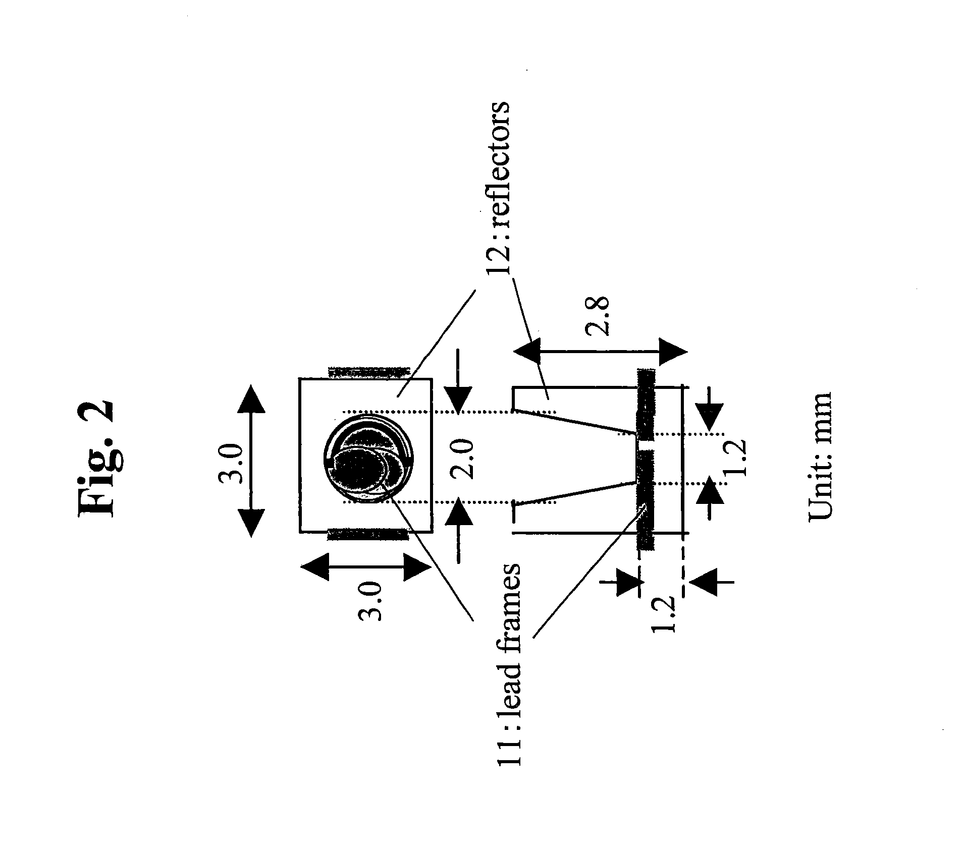
Optical semiconductor sealing material
a technology of optical semiconductor and sealing material, which is applied in the direction of semiconductor device details, adhesive types, semiconductor/solid-state device devices, etc., can solve the problems of resin yellowing, low light output efficiency, and resins that have not yet shown satisfactory properties, and achieve excellent adhesiveness and processability, excellent heat resistance and refractive index compatibility
- Summary
- Abstract
- Description
- Claims
- Application Information
AI Technical Summary
Benefits of technology
Problems solved by technology
Method used
Image

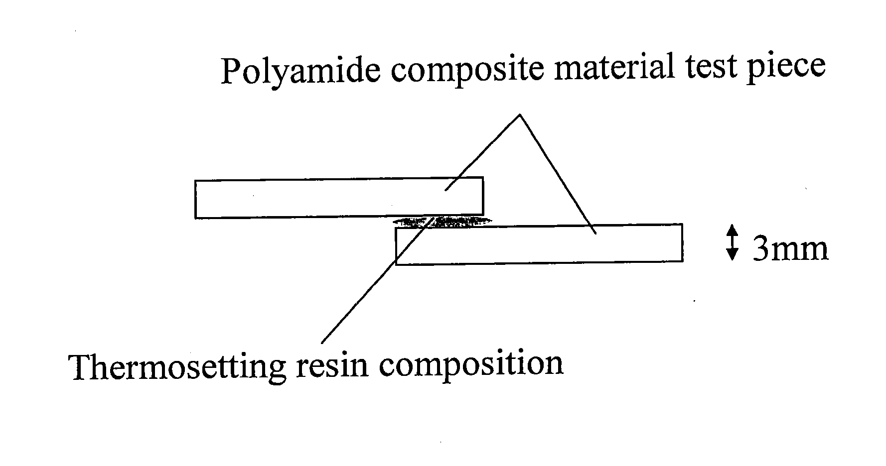
Examples
example 1
[0070]A curable composition was prepared by mixing 21 g of 1-adamantyl methacrylate (made by Idemitsu Kosan Co., Ltd.) with 0.021 g of 1, 1 - bis (t-butylperoxy) -3, 3, 5-trimethylcyclohexane (PERHEXA 3M-95 made by NOF CORPORATION) as a radical polymerization initiator. This composition was fed into a cell that was defined by two glass plates separated by a Teflon spacer with thickness of 3 mm. The cell was heated at 100° C. for 1 hour, 110° C. for 1 hour, 120° C. for 1 hour, and then 130° C. for 30 minutes in an oven, and then gradually cooled to room temperature to form a colorless transparent hardened plate article. The observed properties of the hardened article are shown in Table 1.
example 2
[0071]A hardened article was prepared as in Example 6, except that the monomer was changed to dicyclopentanyl methacrylate (FANCRYL FM-513 made by Hitachi Chemical Company, Ltd.) and the radical polymerization initiator was changed to azobisisobutyronitrile (made by TOKYO CHEMICAL INDUSTRY CO. LTD.) in Example 1. The observed properties of the hardened article are shown in Table 1.
example 3
[0072]A hardened article was prepared as in Example 6, except that the monomer was changed to isobornyl methacrylate (made by Wako Pure Chemical Industries, Ltd.). The observed properties of the hardened article are shown in Table 1.
PUM
| Property | Measurement | Unit |
|---|---|---|
| mass % | aaaaa | aaaaa |
| mass % | aaaaa | aaaaa |
| mass % | aaaaa | aaaaa |
Abstract
Description
Claims
Application Information
 - R&D
- Intellectual Property
- Life Sciences
- Materials
- Tech Scout
- Unparalleled Data Quality
- Higher Quality Content
- 60% Fewer Hallucinations
Browse by: Latest US Patents, China's latest patents, Technical Efficacy Thesaurus, Application Domain, Technology Topic, Popular Technical Reports.
© 2025 PatSnap. All rights reserved.Legal|Privacy policy|Modern Slavery Act Transparency Statement|Sitemap|About US| Contact US: help@patsnap.com