
Liquid crystal display device

a liquid crystal display and display device technology, applied in non-linear optics, instruments, optics, etc., can solve the problems of narrow viewing angle, non-uniform rubbing, and film scraping, and achieve the effect of restricting lateral displacemen

Inactive Publication Date: 2012-10-25
JAPAN DISPLAY INC
View PDF6 Cites 16 Cited by
  • Summary
  • Abstract
  • Description
  • Claims
  • Application Information

AI Technical Summary

Benefits of technology

[0016]The present invention intends to provide a liquid crystal display device of higher quality that can suppress scraping of an alignment film and prevent micro light spot failure.
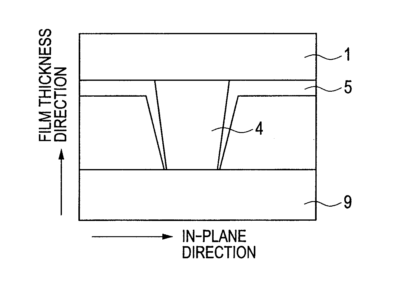
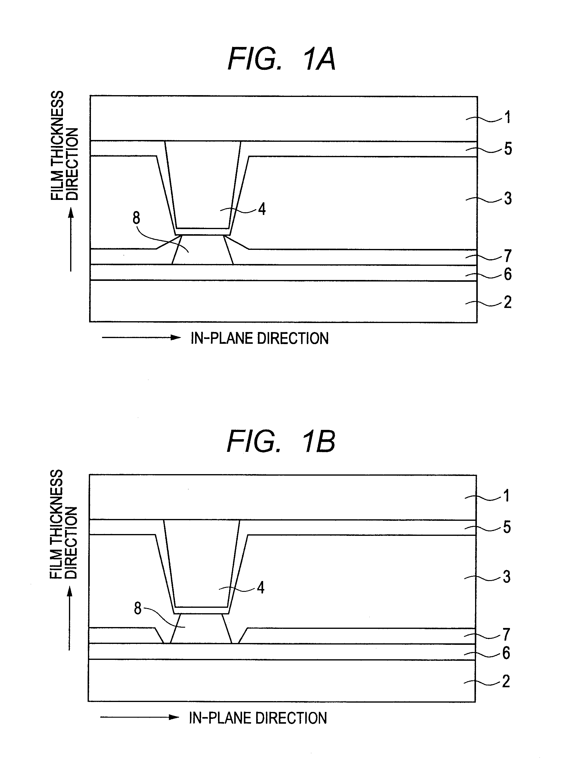
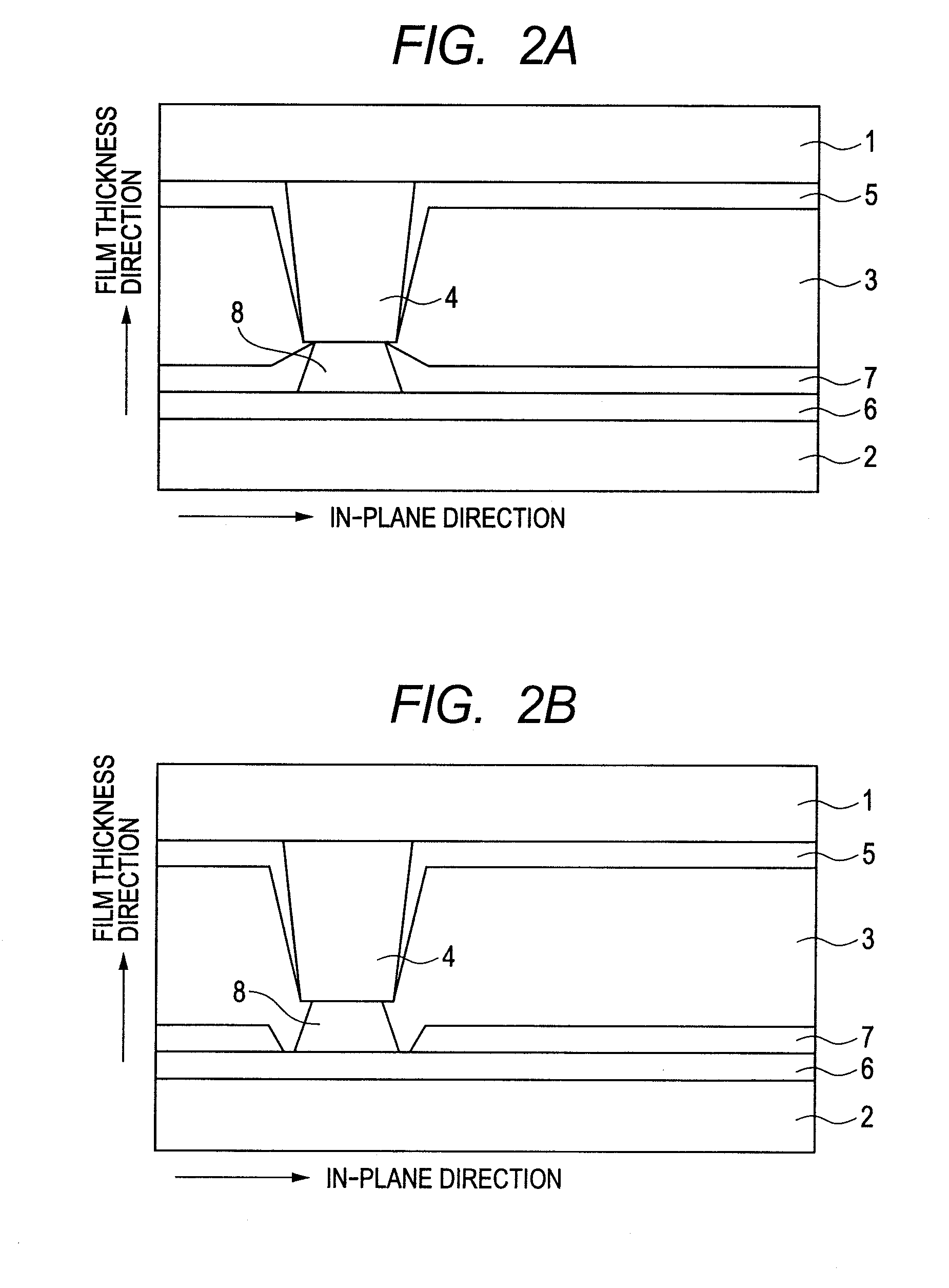
[0020]An aspect of the present invention provides a structure in which a liquid crystal alignment film is not deposited on positions opposing the columnar spacers, which are disposed to keep a constant distance between the upper and lower substrates of the liquid crystal display device. Scraping of the alignment film at the position opposing the columnar spacer caused by contact and lateral displacement can be restricted. As a result, one of the display failures, micro light spots can be prevented from generating.

Problems solved by technology

One major problem of TN and VA liquid crystal display devices is that the view angle is narrow.
However, in rubbing treatments, static electricity or contaminants may be generated by the rubbing, and also the rubbing may be performed non-uniformly due to unevenness of the substrate surface.
Since an alignment film exists at the contact area between the columnar spacer and the receiving pedestal, for reasons such as vibration upon packaging or transportation of the liquid crystal display device, or warpage of the liquid crystal display device caused by a change in its usage temperature circumstance, the contact and friction between the columnar spacer and receiving pedestal the may scrape the film.
The scraped films particularly cause a significant problem regarding the display quality at portions displaying low luminance light (low gradation image) such as black color.
These methods, however, cannot completely suppress generation of scraped films and cannot prevent micro light spot failure.

Method used


Image

  • Liquid crystal display device
  • Liquid crystal display device
  • Liquid crystal display device

Examples


embodiment 1

[0115]At first, a receiving pedestal of an example of a liquid crystal display device according to the invention is to be described with reference to drawings and tables. Here, the examination results of when an IPS panel was manufactured are shown.

[0116]FIG. 13 shows the structure of a receiving pedestal examined in this embodiment. In this embodiment, a receiving pedestal having a square shape in a planer structure was manufactured. It is assumed that the length on one side of the central portion of the pedestal is x, the thickness thereof is z, and the angle between the normal of the substrate surface and the tapered portion of the pedestal is taper angle θ. Specifically, a substrate that has been processed up to a step where elements such as TFT circuits are provided and an insulation film 6 of SiN is formed over the second substrate 2.

[0117]MoCr of z=150 nm was deposited over the insulation layer and the MoCr layer was patterned by using a square photomask pattern of x=5 μm and...

embodiment 2

[0131]Next, an example of a receiving pedestal of another embodiment of a liquid crystal display device of the invention is to be described with reference to the drawing and the table. FIG. 19 shows the layout of a receiving pedestal and light shielding portions of photomasks for partially providing liquid repellency used in Embodiment 2. The receiving pedestal is identical with that of the Embodiment 1, and the same silane coupling agent for providing liquid repellency was coated. However, the pattern of the photomask for partially removing the silane coupling agent was changed from the square shape in the Embodiment 1 to the photomask light shielding regions 9 and 9′ indicated by the two circles.

[0132]That is, while the liquid repellent pattern in the Embodiment 1 was such that no polyamide acid solution of the alignment film would be deposited over the central portion of the receiving pedestal, the Embodiment 2 is characteristic in that the pattern is such that the central portio...

embodiment 3

[0138]FIG. 21 shows an example of another embodiment near the columnar spacer of the invention. While the receiving pedestal 8 was disposed at a position opposing the columnar spacer 4 in the previous embodiments, it is also possible to form a structure of receiving the columnar spacer by not disposing a special receiving pedestal 8 but utilizing already formed members, for example, members such as a transparent electrode, a gate interconnect, a video signal line, a planarizing film, etc.

[0139]In the second substrate, the second alignment film 7 does not exist at a position in contact with the columnar spacer 4. A method of forming a portion where the second alignment film 7 is not present includes: for example, (1) a method of patterning a fluoro alkyl silane; (2) a method of patterning a silane coupling agent by UV-light or the like; and (3) a method of using oxygen plasma or CF4 plasma.

[0140]A transparent conductive film may be present or an insulation layer may be present at a p...


PUM

PropertyMeasurementUnit
temperatureaaaaaaaaaa
thicknessaaaaaaaaaa
heightaaaaaaaaaa

Abstract

Provided is a high quality liquid crystal display device adapted to suppress scraping of alignment film and prevent micro light spot fault. The liquid crystal display device comprises: a plurality of columnar spacers and a first alignment film disposed over a first substrate; an insulation film disposed over a second substrate; and a second alignment film disposed over the insulation layer; receiving pedestals for the columnar spacers, wherein: the second alignment film is not formed over the central portion of each of the receiving pedestals; and around the outer peripheral portion of each receiving pedestal, the second alignment film has an inclined thickness distribution which is such that the thickness thereof increases gradually from the central portion to the outside position of the receiving pedestal.

Description

CLAIM OF PRIORITY[0001]The present application claims priority from Japanese Patent Application JP 2011-095970 filed on Apr. 22, 2011, the content of which is hereby incorporated by reference into this application.BACKGROUND OF THE INVENTION[0002]1. Field of the Invention[0003]The present invention relates to a stable liquid crystal display device of high image quality adapted to prevent generation of micro light spots.[0004]2. Description of the Related Art[0005]Use of liquid crystal display devices has extended due to their advantageous features of high display quality, thinness, light weight, and low power consumption. For example, they are used for portable monitors such as mobile phone monitors and digital still camera monitors, and also for desk top personal computer monitors, monitors for printing and designing, monitors for medical equipment, liquid crystal televisions, etc. Along with the extension of application use, liquid crystal display devices are desired to have highe...

Claims


Application Information

Patent Timeline
Patent Type & Authority Applications(United States)
IPC IPC(8): G02F1/1337
CPCG02F2001/133776G02F1/13394G02F1/133776
Inventor IMANISHI, YASUOSONODA, HIDEHIROKUNIMATSU, NOBORUTOMIOKA, YASUSHIMATSUMORI, MASAKI
Owner JAPAN DISPLAY INC
Learn More