Programmable LSI

Inactive Publication Date: 2012-10-25
SEMICON ENERGY LAB CO LTD
View PDF9 Cites 30 Cited by
  • Summary
  • Abstract
  • Description
  • Claims
  • Application Information

AI Technical Summary

Benefits of technology

[0011]Thus, it is an object to provide a low-power programmable LSI that employs normally off driving and quickly starts. It is an object to provide a programmable LSI that can perform dynamic configuration.
[0014]One aspect of a programmable LSI in the present invention includes a plurality of logic elements. The plurality of logic elements each include a configuration memory, a look-up table, a selection circuit, and a register. In each of the plurality of logic elements, configuration data stored in the configuration memory is input to the look-up table, and the look-up table performs different arithmetic processing in accordance with the configuration data. Configuration data stored in the configuration memory is input to the selection circuit, and the selection circuit changes an electrical connection between the logic elements in accordance with the configuration data. An output signal from the look-up table and a clock signal are input to the register, and the register outputs a signal corresponding to the output signal in synchronization with the clock signal. A storage circuit capable of retaining stored data (configuration data) even after supply of power supply voltage is stopped is used as the configuration memory.
[0017]A storage circuit used as a configuration memory can include a set of volatile and nonvolatile storage circuits. The configuration memory with the structure can store data (configuration data) retained in the volatile storage circuit before supply of power supply voltage is stopped in the nonvolatile storage circuit (hereinafter this operation is also called data storage) in the case where normally off driving is performed. While the supply of power supply voltage is stopped, the data (configuration data) can be retained in the nonvolatile storage circuit (hereinafter this operation is also called data waiting). Then, after supply of power supply voltage is selected, the data (configuration data) retained in the nonvolatile storage circuit is input to the volatile storage circuit (hereinafter this operation is also called data provision), so that the data (configuration data) retained before the supply of power supply voltage is stopped can be retained in the volatile storage circuit again.
[0022]Data is stored in the nonvolatile storage circuit after a signal potential corresponding to the data is input to a predetermined node (the one electrode of the capacitor), the transistor whose off-state current is extremely low is turned off, and the node is set in a floating state. Thus, the nonvolatile storage circuit does not easily cause degradation due to repetitive data rewriting, and rewritability can be improved.
[0025]With the use of the nonvolatile storage circuit, even after supply of power supply voltage is stopped, a configuration memory can continue to retain configuration data for a long time. Thus, after supply of power supply voltage is stopped, writing of configuration data to the configuration memory is not needed when power supply voltage is supplied again, so that the starting time of a programmable LSI can be shortened. Consequently, in the programmable LSI, supply of power supply voltage can be frequently stopped, and power consumption can be markedly reduced by normally off driving.
[0026]In the case where the configuration memory includes a set of volatile and nonvolatile storage circuits, configuration data can be stored in and output from the volatile storage circuit while power supply voltage is supplied. Here, the operation speed of a volatile storage circuit (e.g., a flip-flop circuit or a latch circuit) is high. Thus, the access speed of the configuration memory can be increased. In this manner, a programmable LSI that can perform dynamic configuration can be provided. Further, when a highly reliable circuit whose rewritability is high is used as the nonvolatile storage circuit used in the configuration memory, the durability and reliability of the programmable LSI can be improved.

Problems solved by technology

Here, if a programmable LSI disclosed in Patent Document 1 employs normally off driving, when supply of power supply voltage to the programmable LSI is stopped, configuration data stored in a configuration memory is lost because an SRAM, which is a volatile storage circuit, is used as the configuration memory.
Consequently, after the power supply voltage is supplied again, it takes a long time for the programmable LSI to fulfill its function (to start) (i.e., a starting time is long).
Accordingly, since it takes a long time for the programmable LSI disclosed in Patent Document 1 to start, it is difficult to stop supply of power supply voltage frequently in order to reduce power consumption.
Thus, it is difficult to say that the programmable LSI disclosed in Patent Document 1 is suitable for normally off driving.

Method used


Image

  • Programmable LSI
  • Programmable LSI
  • Programmable LSI

Examples


embodiment 1

[0054]One aspect of a programmable LSI is described.

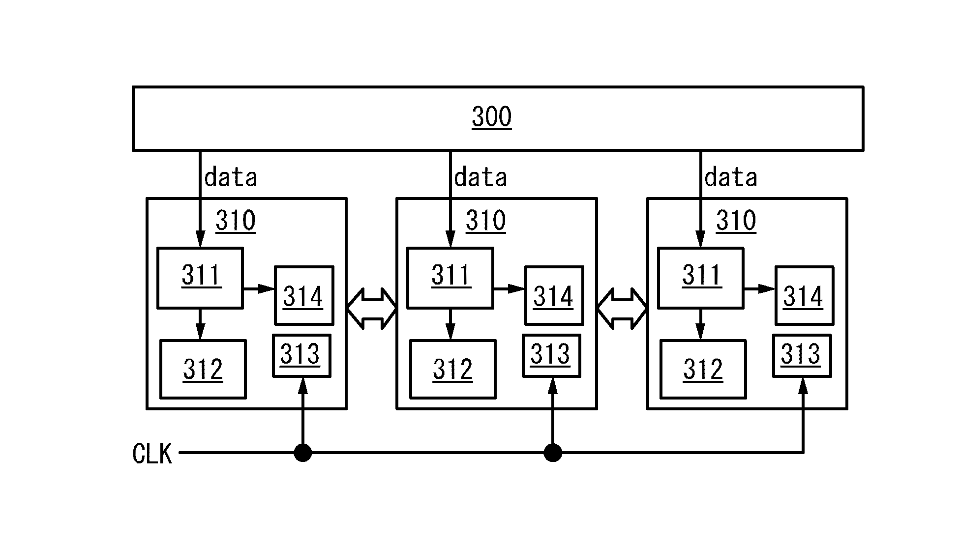
[0055]FIG. 1A schematically illustrates the structure of a programmable LSI. The programmable LSI includes a plurality of logic elements 310 and a memory element 300. FIG. 1A typically illustrates the three logic elements 310. The number of logic elements can be a given number. The programmable LSI may further include plural sets of the plurality of logic elements 310 and the memory element 300. Alternatively, the programmable LSI may further include a multiplier, a RAM block, a PLL block, or an I / O element. The multiplier has a function of multiplying plural pieces of data at high speed. The RAM block functions as a memory for storing given data. The PLL block has a function of supplying a clock signal to a circuit in the programmable LSI. The I / O element has a function of controlling signal passing between the programmable LSI and an external circuit.

[0056]The logic element 310 includes a configuration memory 311, a look-up table...

embodiment 2

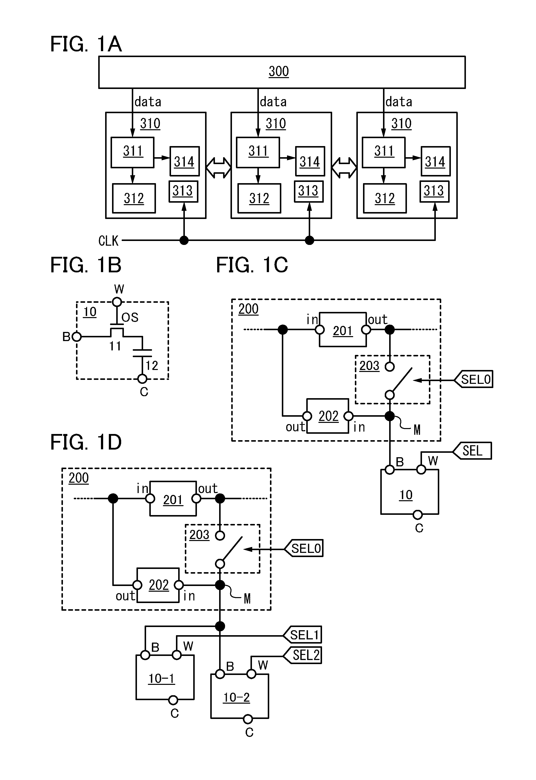
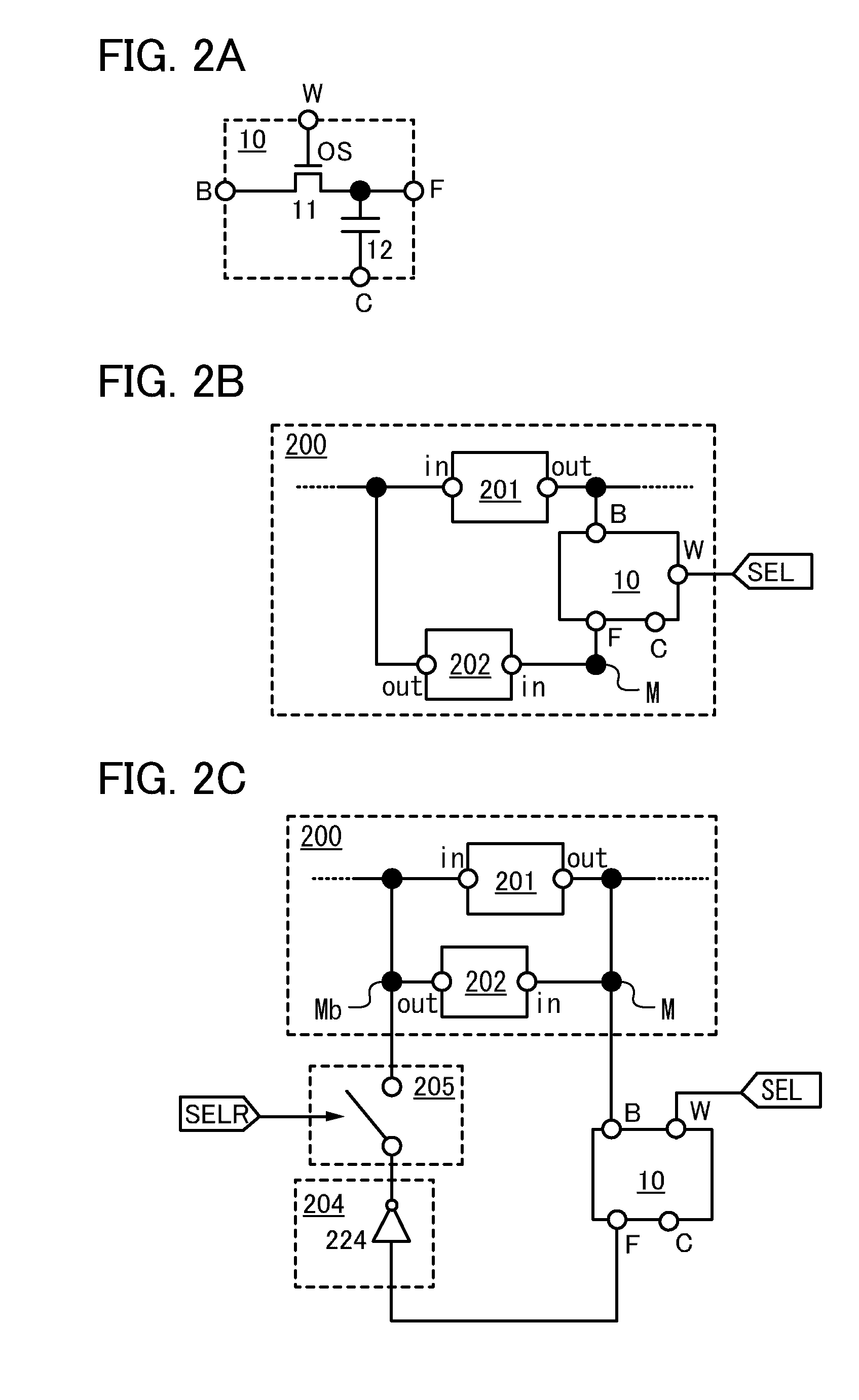
[0099]In this embodiment, a more specific aspect of the memory element 300 is described. The memory element 300 can include a plurality of storage circuits. As a storage circuit used in the memory element 300, it is possible to use a storage circuit (hereinafter referred to as a memory cell) that includes a transistor whose channel is formed in an oxide semiconductor layer and a node that is set in a floating state when the transistor is turned off. FIGS. 5B to 5D illustrate one aspect of the memory cell.

(Structure 1 of Memory Cell)

[0100]A memory cell 100a in FIG. 5B includes a transistor 101, a transistor 102, and a capacitor 103. A channel of the transistor 101 is formed in an oxide semiconductor layer. Note that in FIG. 5B, “OS” is written beside the transistor 101 in order to indicate that the channel of the transistor 101 is formed in the oxide semiconductor layer. A gate of the transistor 101 is electrically connected to a terminal W. One of a source and a drain of the transis...

embodiment 3

[0138]In this embodiment, a more specific aspect of the memory element 300 in Embodiment 2 is described.

[0139]The memory element 300 can include a memory cell array including the plurality of memory cells in Embodiment 2 (having Structure 1 of the memory cell, Structure 2 of the memory cell, or Structure 3 of the memory cell) arranged in matrix.

[0140]The memory element 300 can include any of or all of a decoder (a row decoder or a column decoder), a precharge circuit, a sense amplifier, and a temporary storage circuit in addition to the memory cell array. Note that some of these circuits can be merged into a single circuit. For example, the sense amplifier may function as a temporary storage circuit.

[0141]The decoder (the row decoder or the column decoder) has a function of selecting a given memory cell in the memory cell array. The memory element 300 writes and reads data to and from the memory cell selected by the decoder (the row decoder or the column decoder). The precharge circ...


PUM


Abstract

A low-power programmable LSI that can perform dynamic configuration is provided. The programmable LSI includes a plurality of logic elements. The plurality of logic elements each include a configuration memory. Each of the plurality of logic elements performs different arithmetic processing and changes an electrical connection between the logic elements, in accordance with the configuration data stored in the configuration memory. The configuration memory includes a set of a volatile storage circuit and a nonvolatile storage circuit. The nonvolatile storage circuit includes a transistor whose channel is formed in an oxide semiconductor layer and a capacitor whose one of a pair of electrodes is electrically connected to a node that is set in a floating state when the transistor is turned off.

Description

BACKGROUND OF THE INVENTION[0001]1. Field of the Invention[0002]The present invention relates to semiconductor devices. In particular, the present invention relates to programmable LSIs and semiconductor devices including the programmable LSIs. Further, the present invention relates to electronic devices including the semiconductor devices.[0003]2. Description of the Related Art[0004]Programmable LSIs show flexibility in a reduction in development period and a change in design specification as compared to conventional application specific integrated circuits (ASIC) and gate arrays, which is advantageous. Programmable LSIs are widely used in semiconductor devices.[0005]A programmable LSI includes, for example, a plurality of logic elements and wirings between the logic elements. When the functions of the logic elements are changed, the function of the programmable LSI can be changed. The logic element includes, for example, a look-up table and the like. The look-up table performs ari...

Claims


Application Information

Patent Timeline
IPC IPC(8): H03K19/094
CPCH03K19/17796H01L27/1203H01L27/11803G11C16/0433H03K19/173
Inventor KOBAYASHI, HIDETOMOENDO, MASAMISHIONOIRI, YUTAKADEMBO, HIROKINISHIJIMA, TATSUJIOHSHIMA, KAZUAKIYONEDA, SEIICHIKOYAMA, JUN
Owner SEMICON ENERGY LAB CO LTD
Why Eureka
Try Eureka