
Techniques for Reducing Duty Cycle Distortion in Periodic Signals

a technology of periodic signals and duty cycle distortion, applied in the field of electronic circuits, can solve the problems of adding additional dcd to the output clock signals, generating data dependent jitter in the output data signal of the 2-to-1 multiplexer circuit, and reducing the duty cycle distortion

Inactive Publication Date: 2012-10-11
ALTERA CORP
View PDF1 Cites 8 Cited by
  • Summary
  • Abstract
  • Description
  • Claims
  • Application Information

AI Technical Summary

Benefits of technology

[0013]According to some embodiments, a transmitter circuit is operable to provide an output signal in response to a first periodic signal. A multiplexer circuit is operable to provide a second periodic signal as a selected signal during a first phase of operation. The multiplexer circuit is operable to provide the output signal of the transmitter circuit as the selected signal during a second phase of operation. A sampler circuit is operable to generate first samples of the selected signal during the first phase of operation. The sampler circuit is operable to generate second samples of the selected signal during the second phase of operation. A duty cycle control circuit is operable to adjust a duty cycle of the first periodic signal based on the first and the second samples. In some embodiments, the duty cycle control circuit adjusts a duty cycle of the first periodic signal based on the first and the second samples to reduce duty cycle distortion in the first periodic signal.
[0014]In some embodiments, the second periodic signal is a golden clock signal that is not routed through the transmitter circuit. The first samples generated based on the second periodic signal are not affected by jitter in the output signal of the transmitter circuit. The first samples are compared to the second samples to generate a duty cycle correction value that is used to reduce duty cycle distortion in the first periodic signal.

Problems solved by technology

Duty cycle distortion (DCD) in the output clock signals may cause the 2-to-1 multiplexer circuit to generate data dependent jitter in the output data signal.
Jitter in the output data signal may cause the receiver circuit to sample incorrect data bits in the output data signal.
However, process variations that cause mismatches between the transistors in the fifth and sixth inverter circuits in the buffer circuit may add additional DCD to the output clock signals.
The buffer circuit described above does not prevent this type of DCD in the input clock signals from propagating to the output clock signals.

Method used


Image

  • Techniques for Reducing Duty Cycle Distortion in Periodic Signals
  • Techniques for Reducing Duty Cycle Distortion in Periodic Signals
  • Techniques for Reducing Duty Cycle Distortion in Periodic Signals

Examples


Embodiment Construction

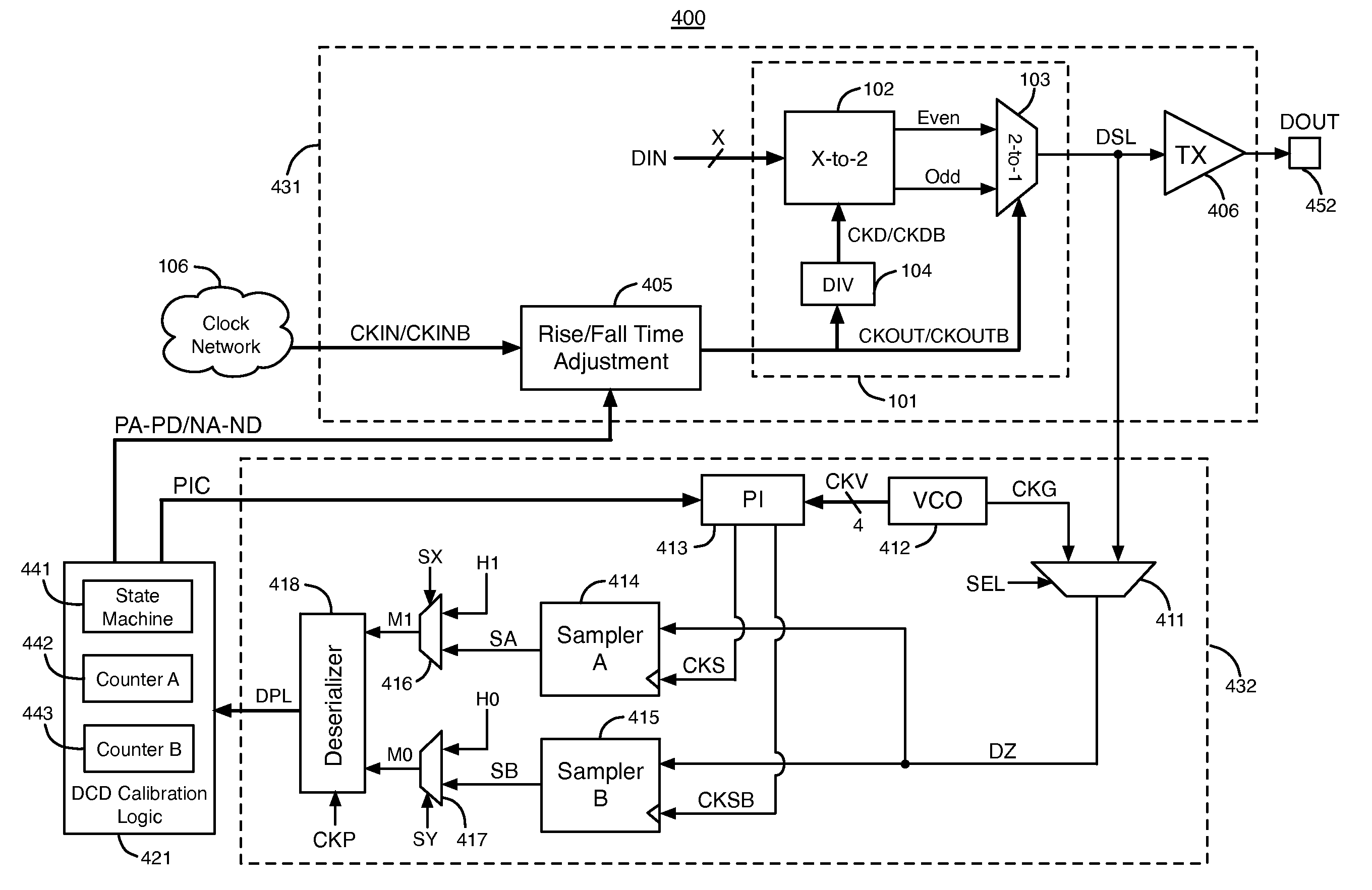
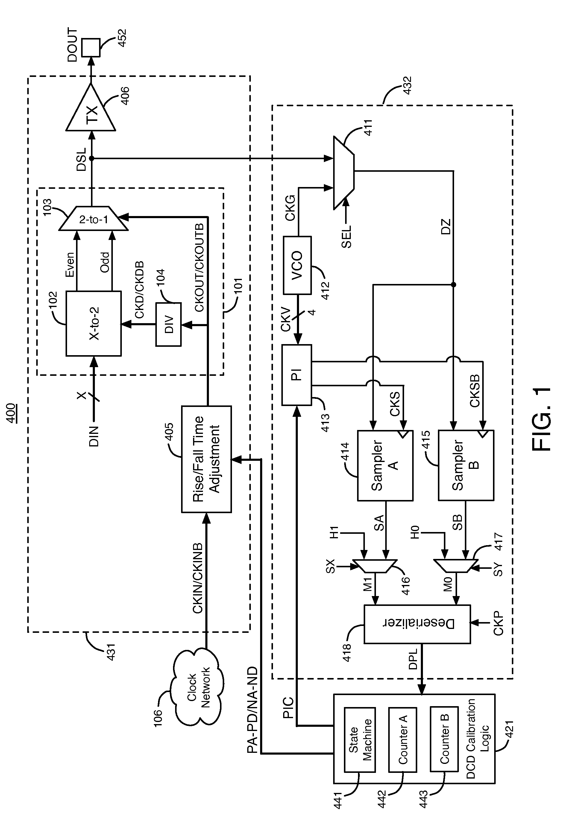
[0023]FIG. 1 illustrates an example of a circuit 400 that compensates for duty cycle distortion (DCD) in two clock signals CKOUT and CKOUTB that are used to generate a serial output data signal, according to an embodiment of the present invention. Circuit 400 includes a transmitter circuit 431, a receiver circuit 432, and duty cycle distortion (DCD) calibration logic circuit 421. Circuit 400 may be in an integrated circuit. The specific components of circuit 400 are exemplary and not intended to limit the scope of the present invention. Many of the specific components of circuit 400 can be replaced with other components to achieve the intended results as described herein.

[0024]Transmitter circuit 431 includes serializer circuit 101, rise / fall time adjustment circuit 405, and transmitter buffer circuit 406. Serializer circuit 101 includes X-to-2 multiplexer circuits 102, a 2-to-1 multiplexer circuit 103, and frequency divider circuit 104. Serializer circuit 101 is merely one example ...


PUM


Abstract

A transmitter circuit is operable to provide an output signal in response to a first periodic signal. A multiplexer circuit is operable to provide a second periodic signal as a selected signal during a first phase of operation. The multiplexer circuit is operable to provide the output signal of the transmitter circuit as the selected signal during a second phase of operation. A sampler circuit is operable to generate first samples of the selected signal during the first phase of operation. The sampler circuit is operable to generate second samples of the selected signal during the second phase of operation. A duty cycle control circuit is operable to adjust a duty cycle of the first periodic signal based on the first and the second samples.

Description

FIELD OF THE INVENTION[0001]The present invention relates to electronic circuits, and more particularly, to techniques for reducing duty cycle distortion in periodic signals.BACKGROUND[0002]One type of conventional transmitter circuit includes a serializer circuit. The serializer circuit includes X-to-2 multiplexer circuits, a 2-to-1 multiplexer circuit, and a frequency divider circuit. An X number of input data signals are provided in parallel to multiplexing inputs of the X-to-2 multiplexer circuit. Parallel data bits are embodied in the input data signals.[0003]Complementary input clock signals are provided through a clock network to inputs of a buffer circuit. The buffer circuit buffers the input clock signals to generate complementary output clock signals that are ideally 180° out of phase. The buffer circuit includes 6 inverter circuits. The first and second inverter circuits in the buffer circuit are connected together in series. The first and second inverter circuits buffer ...

Claims


Application Information

Patent Timeline
Patent Type & Authority Applications(United States)
IPC IPC(8): H03K3/017
CPCH03K5/12H03K3/017H03M9/00H03K5/1565
Inventor DING, WEIQISHUMARAYEV, SERGEYWONG, WILSONHOANG, TIM TRIKE, YANJING
Owner ALTERA CORP
Learn More