
Metal and semimetal sensors near the metal insulator transition regime

a transition regime and metal microbolometer technology, applied in the field of sensors, can solve the problems of short life, high manufacturing cost of cooled microbolometer detectors, and increased manufacturing cost of metal microbolometer detectors, and achieve the effect of improving the sensitivity of metal microbolometers

Inactive Publication Date: 2012-09-06
GAITAS ANGELO
View PDF4 Cites 15 Cited by
  • Summary
  • Abstract
  • Description
  • Claims
  • Application Information

AI Technical Summary

Benefits of technology

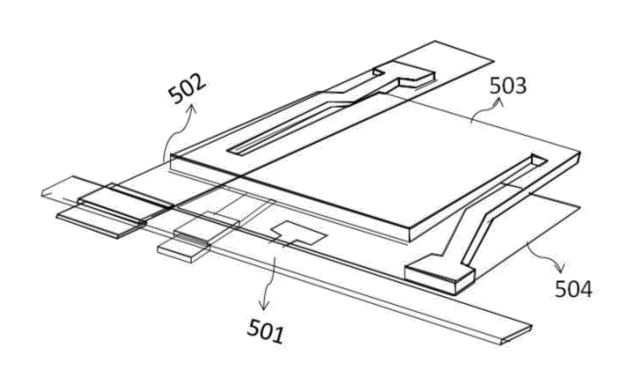
[0013]In one embodiment, intended for scanning thermal microscopy (SThM), an ultrathin film (<20 nm) titanium microbolometer integrated onto a SiO2 / Si3N4 / SiO2 (ONO) cantilever with a Si / SiO2 tip has been fabricated. Wafers with different thicknesses of titanium were also prepared and tested. The morphology of these metal thin films (discontinuous form versus continuous form) [18] is revealed by measuring their electrical properties and atomic force microscopy imaging. Titanium thin film properties near the MIT regime improve the sensitivity of metal microbolometers. Sheet resistances corresponding to the highest TCR and the lowest TCR, in absolute values have been determined. The relationship between TCR and resistance may be typical for many metal, metal oxides, and semimetal thin films near room temperatures. Applications of metal, metal oxides or semimetal films with resistance thicknesses near the MIT can be extended to infrared imaging and chemical sensing. Another object of this invention is to present the design of suspended beam sensors made of granular metallic or semimetallic thin film in the discontinuous phase. These sensors are used either as bolometers or as sensors for sensing movement.

Problems solved by technology

Cooled microbolometer detectors are costly to fabricate, heavier in weight, have shorter lifetimes, low yields, and consume considerably more power than uncooled microbolometers.
Therefore, the thicker, the bolometer film material, the poorer, the overall performance of the imager.
However, vanadium oxide introduces a significant number of deposition problems [6,7,8].
In addition, microbolometers fabricated from vanadium oxides (VOx) and amorphous silicon (a-Si) have been shown to exhibit permanent changes in their electrical properties and in some cases mechanical deformation with a rise in temperature, even if temporary, resulting in changes in TCR values.
The use of pure titanium and its alloys result in a bolometer that occupies a significant amount of space as described in U.S. Pat. No. 5,698,852.
During nucleation, the film is highly susceptible to environmental and deposition conditions and substrate surface conditions.
A small change in distance between the grains due to bending, results in a large change in resistance of the film.

Method used


Image

  • Metal and semimetal sensors near the metal insulator transition regime
  • Metal and semimetal sensors near the metal insulator transition regime
  • Metal and semimetal sensors near the metal insulator transition regime

Examples


Embodiment Construction

[0033]The object of the present invention is to provide a method for fabrication of an uncooled microbolometer from thin films of metals and semimetals close to the metal insulator transition (MIT) regime and / or near the metal semiconductor transition (MST) regime. Another object of the present invention is to fabricate a microbolometer that attains the maximum temperature coefficient of resistance (TCR) near the metal insulator transition (MIT) regime. Yet, another object of the invention is to present the design of suspended beam sensors made of granular metallic or semimetallic thin film in the discontinuous phase. These sensors are used either as bolometers or as displacement sensors.

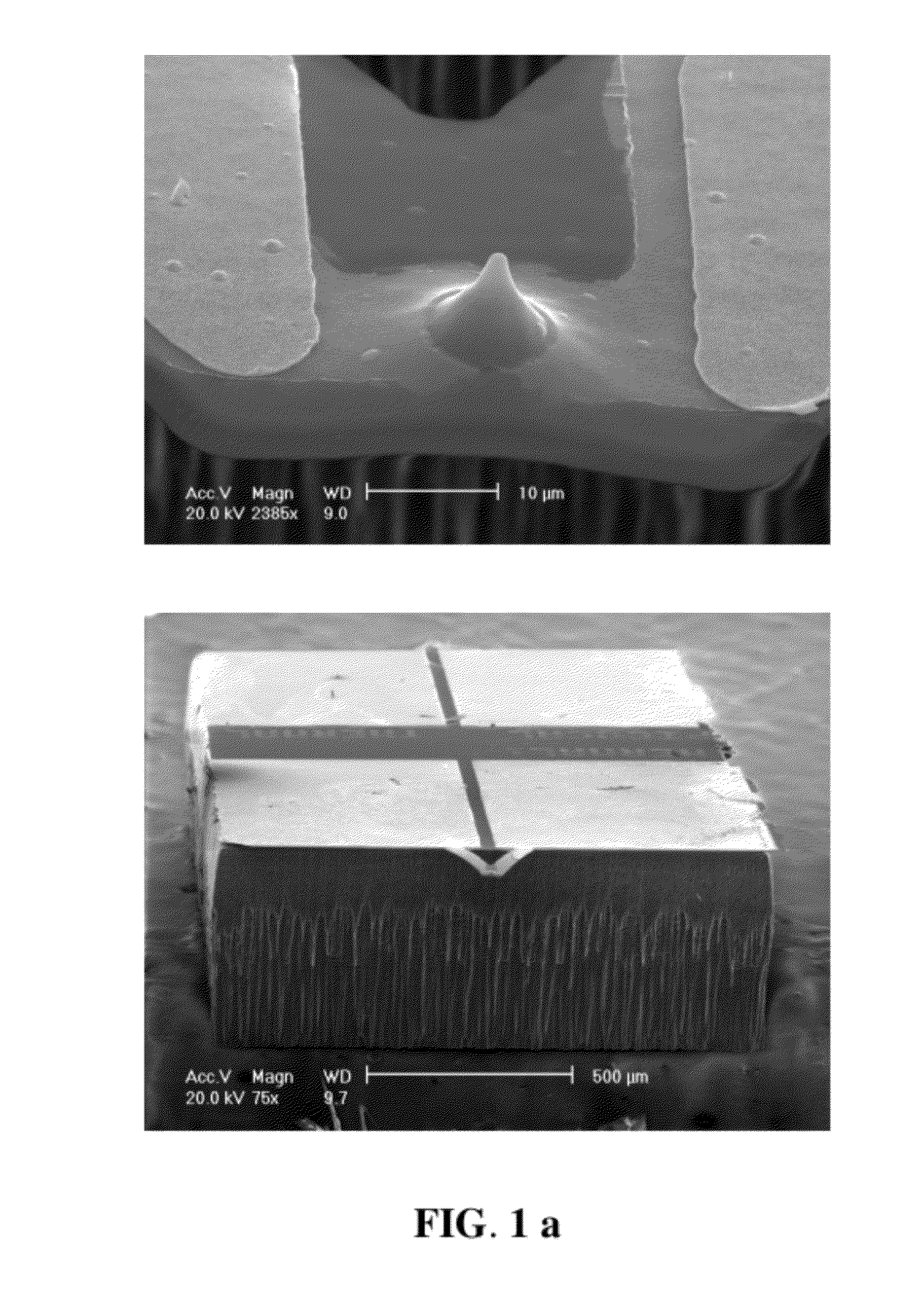
[0034]Referring now to the drawings, more particularly to FIG. 1a, which shows a scanning electron micrograph (SEM) of a microbolometer probe. In this embodiment of the present invention, the cantilevers were made from a 1.1 μm thick SiO2 / Si3N4 / SiO2 (ONO) layer with 10 μm long Si / SiO2 tips. A sensin...


PUM


Abstract

This invention generally relates to sensors made of granular thin films in the discontinuous phase. More particularly, the invention relates to microbolometers and displacement sensors fabricated from thin films that are close to the metal insulator transition (MIT) or metal semiconductor transition (MST) regime. Sensors of various designs have been fabricated according to the invention and may be used for deflection measurements, nano-indentation, visco-elastic measurements, topographical scanning, explosive detection, low abundance biomolecular detection, electromagnetic radiation detection and other similar detection and measurement systems.

Description

TECHNICAL FIELD OF THE INVENTION[0001]This invention generally relates to sensors made of granular metallic or semimetallic thin films in the discontinuous phase. More particularly, the invention relates to uncooled microbolometers and displacement sensors fabricated from thin films that are close to the metal insulator transition (MIT) or metal semiconductor transition (MST) regime.BACKGROUND OF THE INVENTION[0002]Monitoring devices with embedded infrared sensors and detectors are frequently used for video surveillance of people and premises, fire detection, emergency responses, and various other applications where there is a need for such sensors and detectors. Detectors generally operate by detecting the differences in the thermal radiance of various objects in a particular scene. These differences in thermal radiation are converted into electrical signals which are processed, analyzed, and displayed as images in the case of video imager's and noise signals for detectors.[0003]Th...

Claims


Application Information

Patent Timeline
IPC IPC(8): H01C1/012
CPCH01C7/006H01C17/06533H01C17/06526H01C7/06G01Q60/58
Inventor GAITAS, ANGELO
Owner GAITAS ANGELO
Learn More