Electron Microscope
a technology of electron microscope and electron microscope, which is applied in the direction of material analysis using wave/particle radiation, instruments, nuclear engineering, etc., can solve the problems of beam drift phenomenon, non-uniform charging potential on the sample surface, and various types of image degradation, so as to achieve the effect of minimizing blur
- Summary
- Abstract
- Description
- Claims
- Application Information
AI Technical Summary
Benefits of technology
Problems solved by technology
Method used
Image
Examples
first embodiment
[0044]Embodiments of the present invention will be described referring to the drawings.
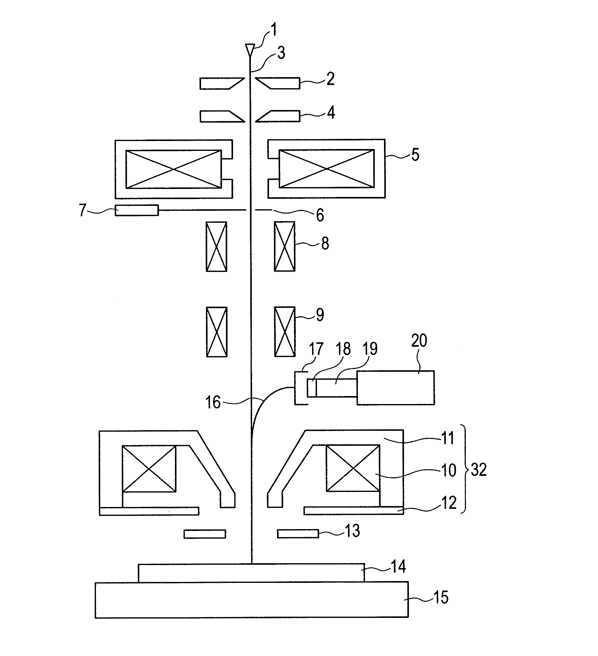
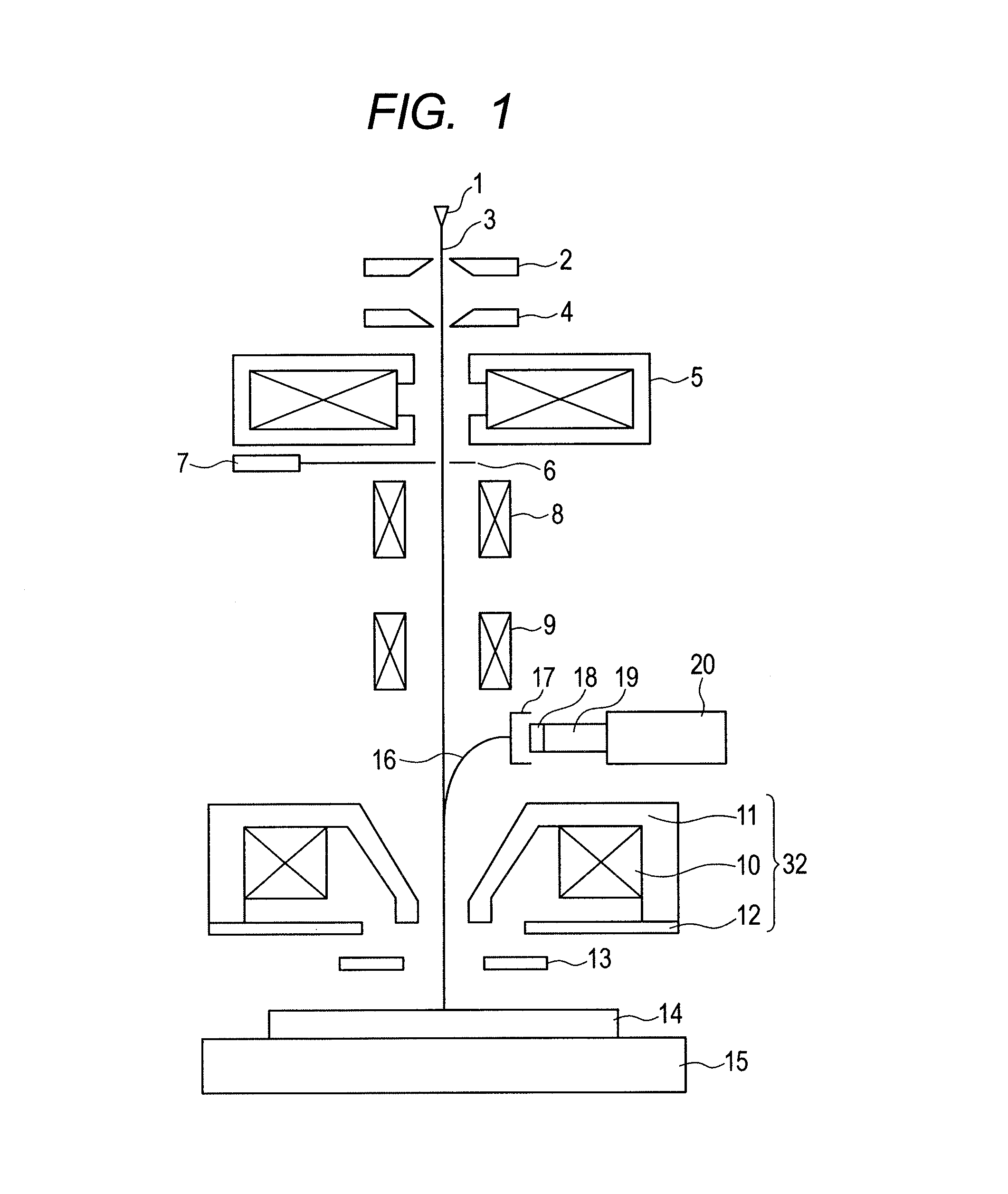
[0045]FIG. 1 is a schematic view of an electron microscope according to an embodiment. This embodiment is intended to conduct measurement and inspection of the interconnection on the wafer with respect to a large sample such as a semiconductor wafer under the condition where energy of a primary electron beam is set at low acceleration voltage ranging from several 100 eV to several keV. The present invention is applicable to the electron microscope irrespective of larger intended sample or object, and higher acceleration voltage so long as it has the similar structure.
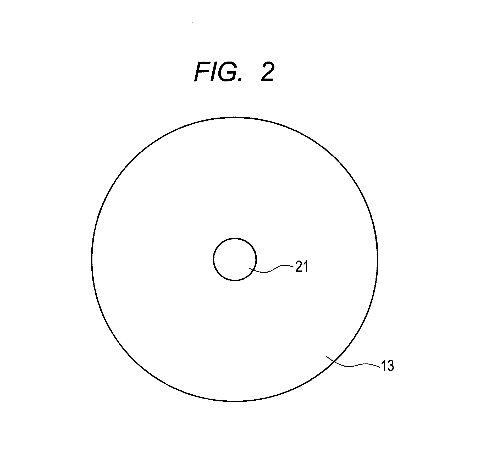
[0046]When applying an extraction voltage between a field emission cathode 1 and an extraction electrode 2 as an electron source, an emitted electron 3 is released. The emitted electron 3 is further accelerated between the extraction electrode 2 and an anode 4 at a ground potential. Energy (acceleration voltage) of the electron beam p...
second embodiment
[0060]A second embodiment will be described referring to FIG. 9. The description of the first embodiment is applicable to this embodiment unless the circumstances are exceptional.
[0061]FIG. 9 illustrates a structure in which a non-magnetic body 30 is further disposed underneath the magnetic body 13 between the objective lens 32 and the sample 14. The sample 14 is held on the sample holder 15. The magnetic body 13 and the non-magnetic body 30 may be made conductive for the purpose of applying the same voltage, or may be insulated for the purpose of applying different voltage. The non-magnetic body 30 is disposed parallel to the sample holder 15, and is made larger than the magnetic body 13 so as to allow controlling of the potential on the sample surface. The non-magnetic body 30 functions to make it difficult to charge the insulating sample as well as suppress the beam drift by reducing the potential gradient on the sample surface.
[0062]FIGS. 10A and 10B schematically show equipoten...
third embodiment
[0065]In the second embodiment, the non-magnetic body is disposed underneath the magnetic body. Such structure increases a working distance between the objective lens and the sample, and the principal plane of the objective lens is far from the sample, thus degrading the resolution. The aforementioned problem may be solved by forming a trench in the non-magnetic body for storage of the magnetic body. FIGS. 13A and 13B illustrate the structure in which the trench is formed in the non-magnetic body for storage of the magnetic body. FIG. 13A illustrates that the trench is formed in the upper side of the non-magnetic body. FIG. 13B illustrates that the trench is formed in the lower side of the non-magnetic body. The structure having the magnetic body fit in the trench provides the advantage of suppressing the resolution degradation by reducing the working distance as well as improvement of the electrode positioning precision. In Embodiments 2 and 3, three electrodes (upper pole piece, m...
PUM
 Abstract
Description
Claims
Application Information
 - R&D
- Intellectual Property
- Life Sciences
- Materials
- Tech Scout
- Unparalleled Data Quality
- Higher Quality Content
- 60% Fewer Hallucinations
Browse by: Latest US Patents, China's latest patents, Technical Efficacy Thesaurus, Application Domain, Technology Topic, Popular Technical Reports.
© 2025 PatSnap. All rights reserved.Legal|Privacy policy|Modern Slavery Act Transparency Statement|Sitemap|About US| Contact US: help@patsnap.com


