Nitride semiconductor substrate and method of manufacturing the same

Active Publication Date: 2012-08-23
COORSTEK INC
View PDF2 Cites 5 Cited by
  • Summary
  • Abstract
  • Description
  • Claims
  • Application Information

AI Technical Summary

Benefits of technology

[0015]Such a structure provides a nitride semiconductor substrate which allows both the higher threshold voltage and current collapse improvement and is suitable for a normally-off type high breakdown voltage device.

Problems solved by technology

On the other hand, the technology described in JP-A No. 2001-196575 is effective in improvement in a pinch off property, but it is not necessarily sufficient in respect of improvement in the threshold voltage and current collapse.
Further, although JP-A No. 2008-010803 discloses that the technology can control the threshold voltage, it still does not sufficiently correspond to a need for obtaining a higher threshold voltage.
Furthermore, the technology described in JP-A No. 2010-123899 can control the current collapse, but it is not sufficient in respect of the improvement in the threshold voltage.

Method used


Image

  • Nitride semiconductor substrate and method of manufacturing the same
  • Nitride semiconductor substrate and method of manufacturing the same
  • Nitride semiconductor substrate and method of manufacturing the same

Examples


experiment 1

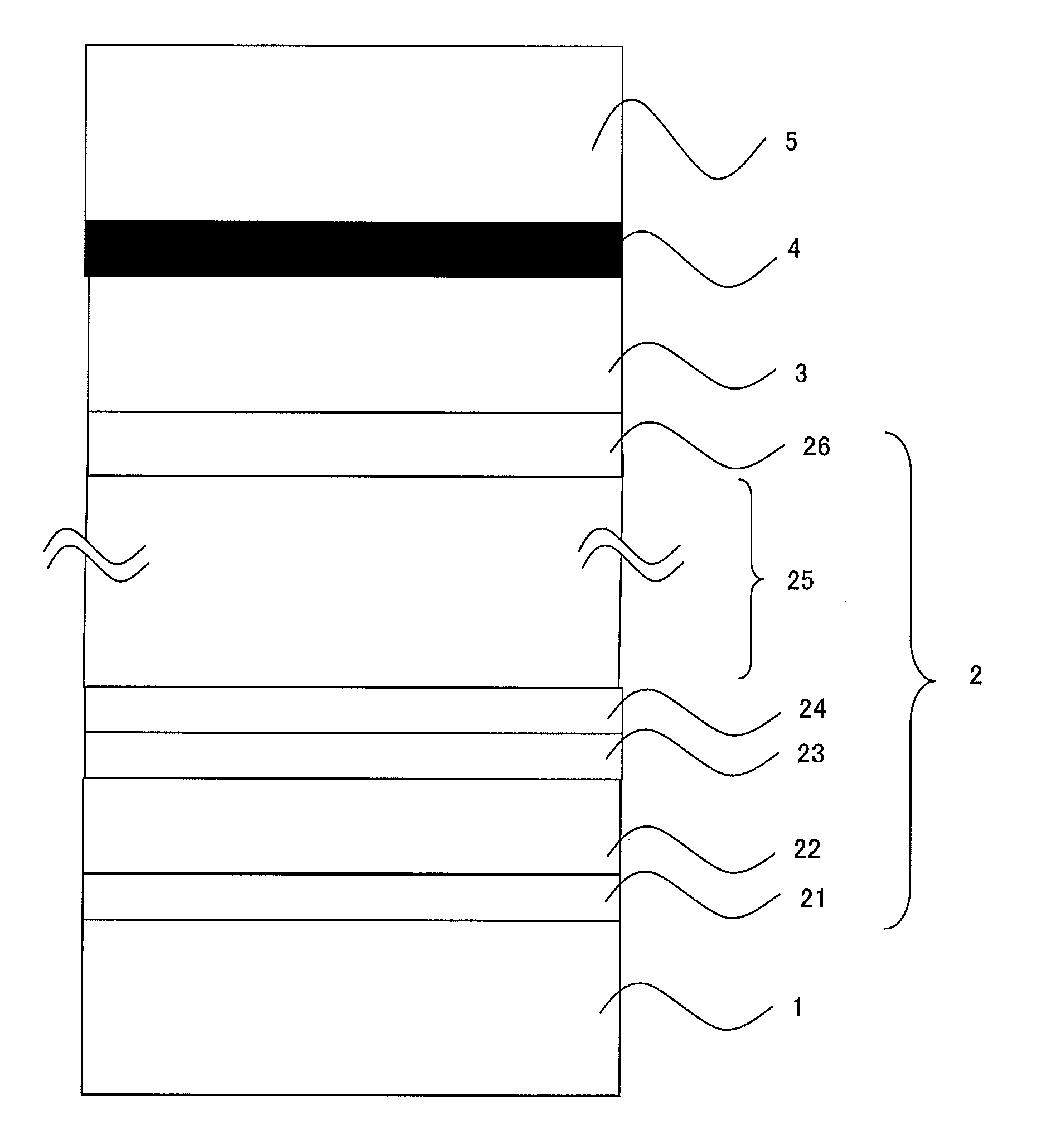
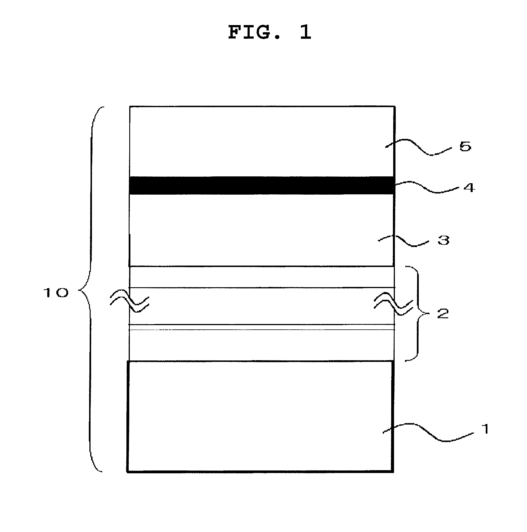
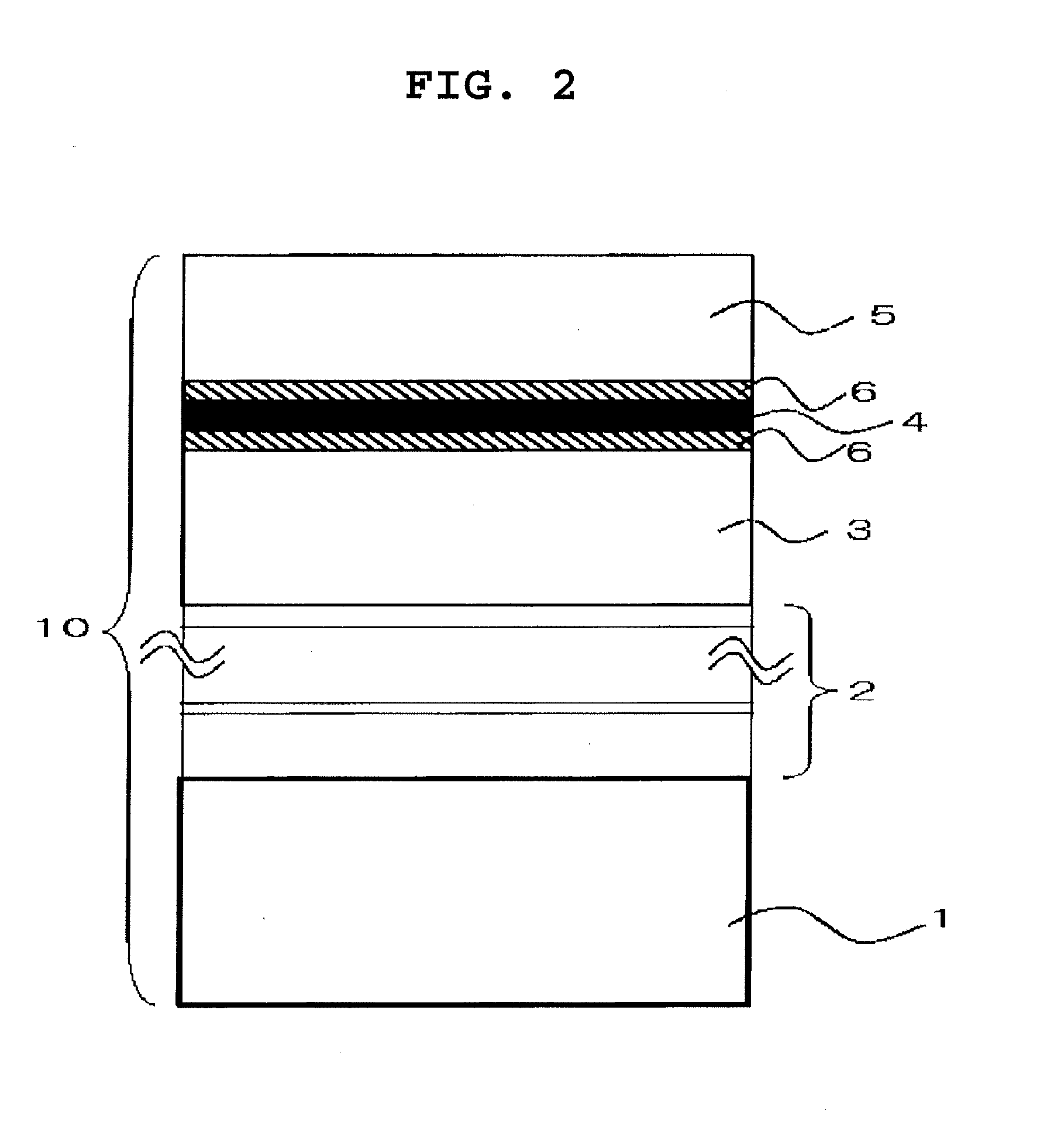
[0071]A nitride semiconductor substrate 10 having a layer structure as shown in FIG. 1 was fabricated according to the following processes. As a common manufacture method, the substrate 1 made of a Si single crystal with a diameter of 3 inches, an n dopant type, a thickness of 625 μm, and a plane direction (100) was placed in an MOCVD apparatus. As materials for the nitride semiconductor, trimethyl gallium (TMG), trimethyl aluminum (TMA), ammonia (NH3), and methane (CH4) were used. According to the layer to, be formed, these materials were used selectively and suitably, and a vapor deposition temperature was raised to 1000° C. to form each layer. In addition, composition and adjustment of a thickness of each layer were achieved by selection of the materials and adjustment of a flow rate, prebsure, and supply time.

[0072]An Aln single crystal layer was formed on the substrate 1 to have a carbon concentration of 5×10¹⁹ atoms / cm3 and a thickness of 20 nm. Subsequently, an Al0.2Ga0.8N si...

experiment 2

[0080]The Al content, the film thickness, and the carbon concentration of the intermediate layer 3 and the film thickness and the carbon concentration of the electron transport layer 4 were changed. Except for these, the nitride semiconductor substrate 10 was fabricated similarly to Sample 1 and evaluated.

[0081]Fabrication conditions and evaluation results are shown in the following table 1. In addition, of properties other than the above-mentioned two evaluation criteria, those changed somewhat are listed in the remarks column. Further, as for several samples, X-ray rocking curve half-value widths are listed for reference.

[0082]The breakdown voltages were evaluated using the curve tracer. One that was 150V per micrometer or more was judged to be “good” on the basis of the breakdown voltage value in Sample 1, and one that was less than it was judged to be “reduced”.

[0083]Further, as for the current collapse, compared with Sample 1, in the case where the current value after applying ...

experiment 3

[0084]The buffer layer 2 was arranged to have a structure as set forth below. Except this, the nitride semiconductor substrate 10 was fabricated similarly to Sample 1 to obtain Sample 30.

[0085]The buffer layer 2 in Sample 30 was provided with an initial buffer layer and repeatedly deposited layers. First, as an initial buffer layer, an Aln single crystal layer was stacked to have a thickness of 100 nm, and an Al0.1Ga0.9N single crystal layer was stacked to have a thickness of 200 nm. Then, as the repeatedly deposited layers, a GaN single crystal layer was formed to have a thickness of 25 nm; subsequently an Aln single crystal layer was stacked to have a thickness of 5 nm. After repeating these operations alternately by way of the similar process to stack a total of 12 layers including six layers each, another GaN layer was formed to have a thickness of 220 nm. Assuming these to be one set of composite layers, six sets were repeatedly stacked.

[0086]Further, in Sample 30, the plane di...


PUM


Abstract

A nitride semiconductor substrate suitable for a normally-off type high breakdown-voltage device and a method of manufacturing the substrate are provided allowing both a higher threshold voltage and improvement in current collapse.In a nitride semiconductor substrate 10 having a substrate 1, a buffer layer 2 formed on one principal plane of the substrate 1, an intermediate layer 3 formed on the buffer layer 2, an electron transport layer 4 formed on the intermediate layer 3, and an electron supply layer 5 formed on the electron transport layer 4, the intermediate layer 3 has a thickness of 200 nm to 1500 nm and a carbon concentration of 5×10¹⁶ atoms / cm3 to 1×10¹⁸ atoms / cm3 and is of AlxGa1-xN (0.05≦x≦0.24), and the electron transport layer 4 has a thickness of 5 nm to 200 nm and is of AlyGa1-yN (0≦y≦0.04).

Description

BACKGROUND OF THE INVENTION[0001]1. Field of the Invention[0002]The present invention relates to a nitride semiconductor substrate for a nitride semiconductor suitable as a high speed and high breakdown-voltage electron device.[0003]2. Description of the Related Art[0004]Nitride semiconductors, such as gallium nitride (GaN), aluminum nitride (AlN), etc., have outstanding properties, such as high electron mobility, high heat resistance, etc., and therefore can suitably be applied to a high electron mobility transistor (HEMT: High Electron Mobility Transistor), a heterojunction field effect transistor (HFET: Heterojunction Field Effect Transistor), for example.[0005]In particular, there is an increasing demand for improvement in various electrical properties in a normally-off type HEMT structure in which a nitride semiconductor is used. In order to cope with this demand, several technologies are known.[0006]For example, Japanese Patent Application Publication No. 2001-196575 discloses...

Claims


Application Information

Patent Timeline
IPC IPC(8): H01L29/20H01L21/20
CPCH01L21/0237H01L21/02458H01L21/02505H01L29/7787H01L21/0262H01L29/2003H01L21/0254
Inventor YOSHIDA, AKIRAKOMIYAMA, JUNABE, YOSHIHISAOISHI, HIROSHIERIGUCHI, KENICHISUZUKI, SHUNICHI
Owner COORSTEK INC
Why Eureka
Try Eureka