Enhanced separation of injection molded microlenses for high volume manufacturing

a microlense and manufacturing technology, applied in the field of injection molding objects, can solve the problems of difficult removal of disadvantageous to the overall production process of optical devices, and difficulty in removing newly formed optical devices from moldplate cavities, etc., to achieve rapid curing of optical materials, facilitate expedient removal of optical devices, and control the effect of differential thermal expansion

Inactive Publication Date: 2012-08-16
IBM CORP
View PDF2 Cites 1 Cited by
  • Summary
  • Abstract
  • Description
  • Claims
  • Application Information

AI Technical Summary

Benefits of technology

[0005]In view of the foregoing disadvantages and other considerations, an embodiment of the present application overcomes the existing problems and facilitates expeditious removal of optical devices from a moldplate by rapidly curing the optical material with intense ultra violet (UV) light pulses, which promotes a controlled differential thermal expansion between the optical device material and the moldplate material. This differential thermal expansion causes the optical material to naturally contract away from the moldplate material due to shrinkage of the optical device material which occurs at a higher rate than a shrinkage of the moldplate material. Preliminary experimental data indicate that if an appropriate optical-grade polymer material is exposed to relatively intense (e.g., 3-4 W) pulses of UV light, the polymer optical material shrinkage occurs very quickly and can be on the order of several percent in volume of the optical material. The polymer shrinkage is sufficiently uniform and does not affect the profile of the optical device. In the injection molding of microlenses, for example, an at least 1% shrinkage can cause the microlenses to separate from the moldplate cleanly without the need for additional mechanical dislodging. As a result, using this approach, a large number of optical devices can be cured and demolded in a single processing step, rather than requiring multiple steps as in conventional approaches. In addition, by using this approach, it is possible to use a thinner coating of release layer for most optical device geometries, or to eliminate the need for the release layer in at least some optical device geometries. Accordingly, this approach not only simplifies the molding process and reduces cost, but also allows for the moldplates to be reused as may times as desired, barring mechanical damage during handling, without having to replace the conformal coat of release layer.

Problems solved by technology

However, some complications of the injection molding process are burning or scorching of parts due to melt temperature being too high or curing cycle time being too long; warping of parts due to uneven surface temperature of the moldplate cavities; surface imperfections and bubbles due to incomplete filling, surface cracking due to rapid change of temperature, and the like.
More importantly, in the injection molding of optical devices, removing the newly formed optical device from the moldplate cavities is often difficult, in particular if the optical material remains adhered to the walls of the cavities.
Thus, the conventional “demolding” process and recoating of the moldplate is disadvantageous to the overall optical device production process due to potential damage that the demolding mechanical apparatuses may cause to the surfaces of the optical devices and / or to the surfaces of the moldplate.
Moreover, the time and expense required for applying a new coat of release layer can render the injection molding process excessively costly.

Method used


Image

  • Enhanced separation of injection molded microlenses for high volume manufacturing
  • Enhanced separation of injection molded microlenses for high volume manufacturing
  • Enhanced separation of injection molded microlenses for high volume manufacturing

Examples


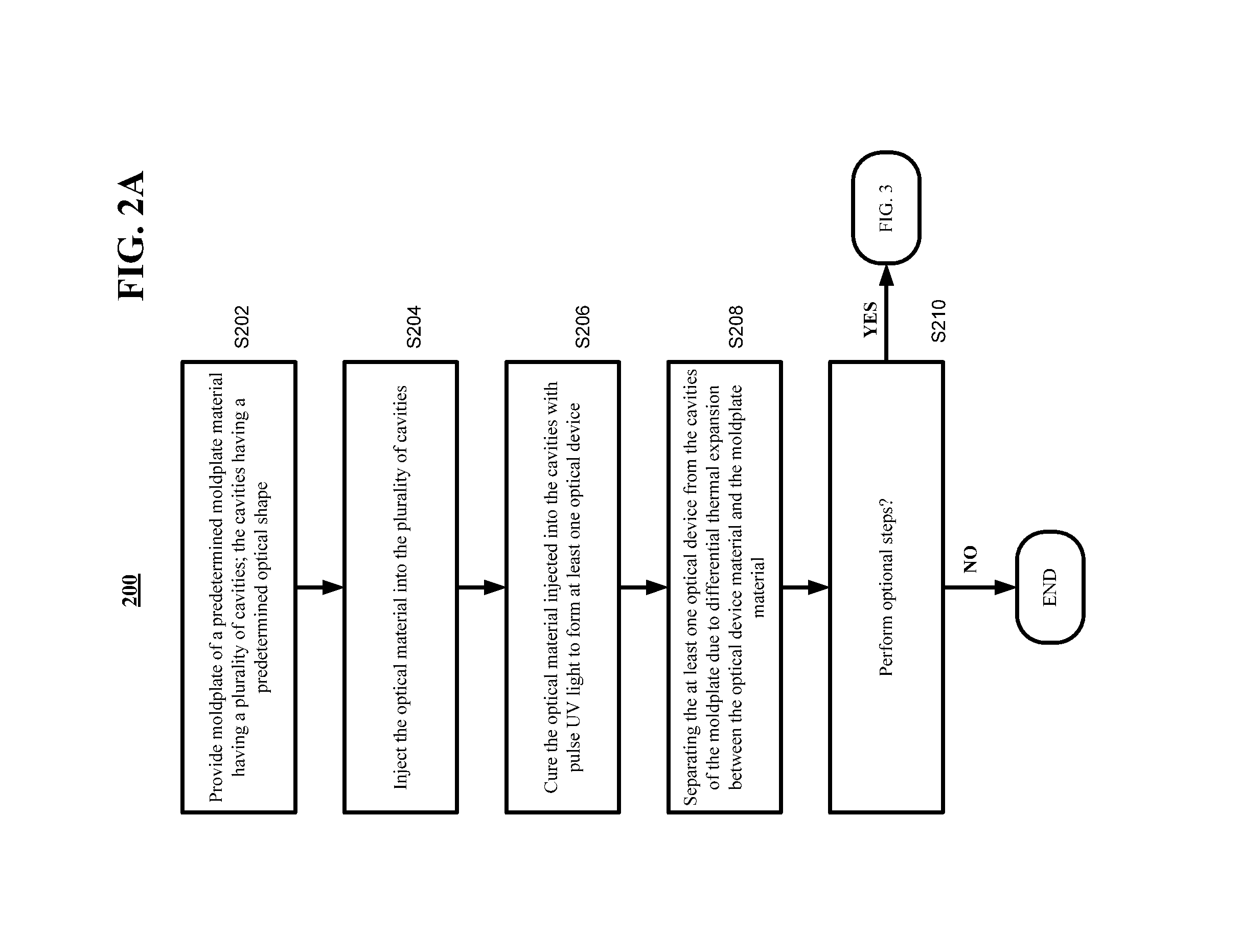
Embodiment Construction

[0016]The terminology used herein is for the purpose of describing particular embodiments only and is not intended to be limiting of the invention. As used herein, the singular forms “a”, “an” and “the” are intended to include the plural forms as well, unless the context clearly indicates otherwise. It will be further understood that the terms “comprises” and / or “comprising,” when used in this specification and claims, specify the presence of stated features, integers, steps, operations, elements, and / or components, but do not preclude the presence or addition of one or more other features, integers, steps, operations, elements, components, and / or groups thereof. In the following description, reference is made to the accompanying drawings where like reference numerals refer to like parts throughout the disclosure.

Thermal Expansion

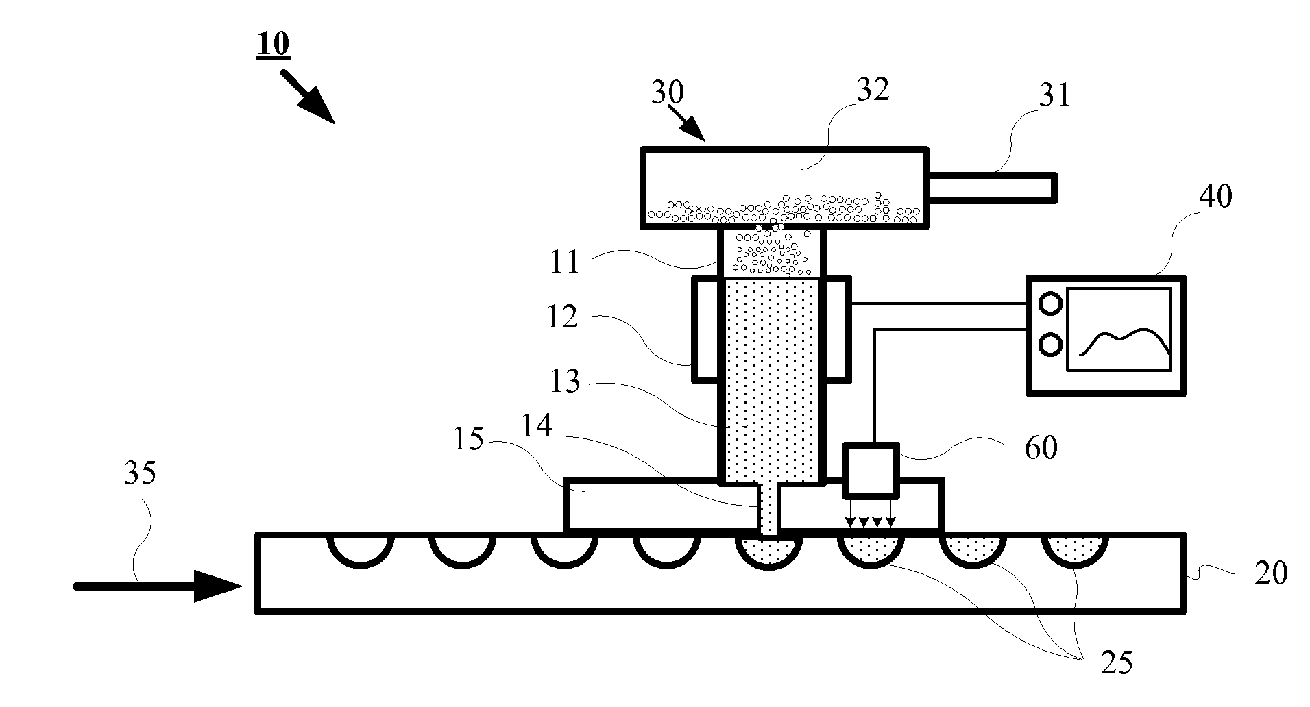
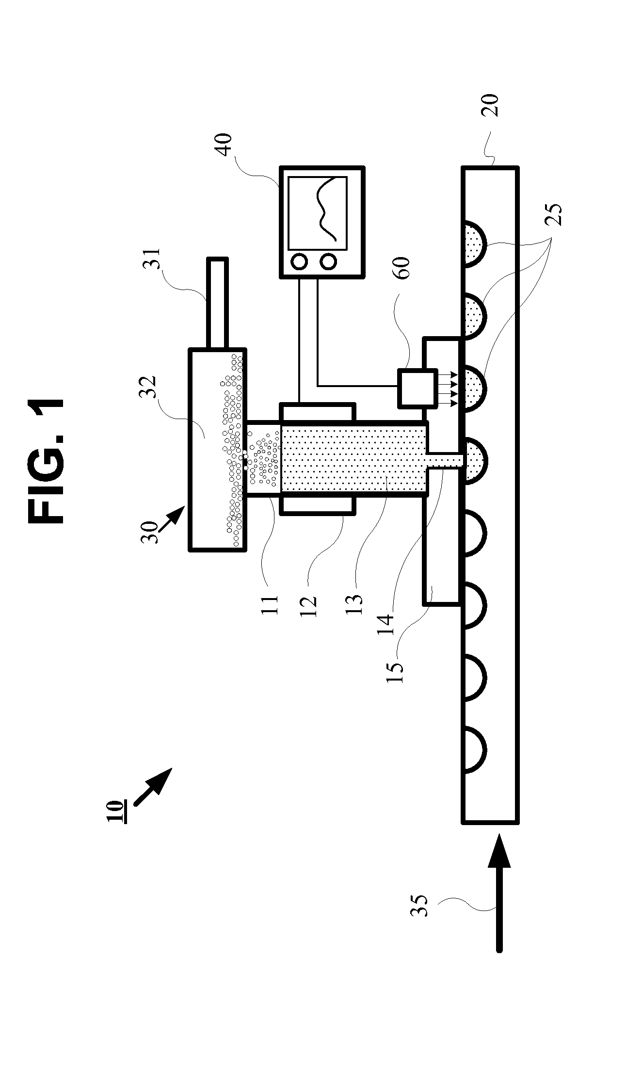
[0017]Because the embodiments of the present invention are partly based on the concept of thermal expansion, it is convenient to discuss such a concept bef...


PUM

PropertyMeasurementUnit
shrinkageaaaaaaaaaa
temperatureaaaaaaaaaa
CTEaaaaaaaaaa

Abstract

A method and system for enhanced demolding of injection molded optical devices are disclosed. In one embodiment the system includes a metal moldplate without a coat of release layer and a curing device that generates high intensity pulses of UV light. The method includes: providing a moldplate made of a predetermined moldplate material; directly injecting optical material into cavities of a moldplate without a release layer; rapidly curing the injected optical material with high intensity pulses of UV light such that a predetermined optical device is formed; and separating the thus formed optical device from the cavities of the moldplate due to a differential thermal expansion between the optical device material and the moldplate material.

Description

CROSS-REFERENCE TO RELATED APPLICATIONS[0001]This application is a divisional application claiming priority under 35 U.S.C. §120 to U.S. patent application Ser. No. 12 / 603,565 filed Oct. 21, 2009, the entire text of which is specifically incorporated by reference herein.FIELD OF INVENTION[0002]The present invention relates to injection molding of objects, and more specifically, to a method and system for enhanced separation of injection molded optical devices from a moldplate. The optical devices are preferably in the micro or nanometer scale.BACKGROUND OR RELATED ART[0003]Injection molding is a manufacturing process for producing parts by feeding material (typically a polymer) into a heated barrel, whereby the material is heated to an appropriate melting temperature and forced into a mold cavity where the material cools and hardens to the configuration of the mold cavity. Injection molding of optical devices, such as lenses, filters or optical waveguides, includes injecting an opti...

Claims


Application Information

Patent Timeline
Patent Type & Authority Applications(United States)
IPC IPC(8): B29C45/03B29C35/08
CPCB29C33/44B29C35/0888B29C37/0003B29D11/00365B29C2035/0827B29D11/00201B29C37/0067B29C37/005B29C2035/0833B29D11/00298
Inventor DECUSATIS, CASIMER M.JACOBOWITZ, LAWRENCE
Owner IBM CORP
Why Eureka
Try Eureka