
Method and system to predict lithography focus error using simulated or measured topography

a lithography and focus error technology, applied in the field of semiconductor fabrication, can solve problems such as the computation of the focus error value of the chip

Inactive Publication Date: 2012-08-02
IBM CORP
View PDF2 Cites 21 Cited by
  • Summary
  • Abstract
  • Description
  • Claims
  • Application Information

AI Technical Summary

Benefits of technology

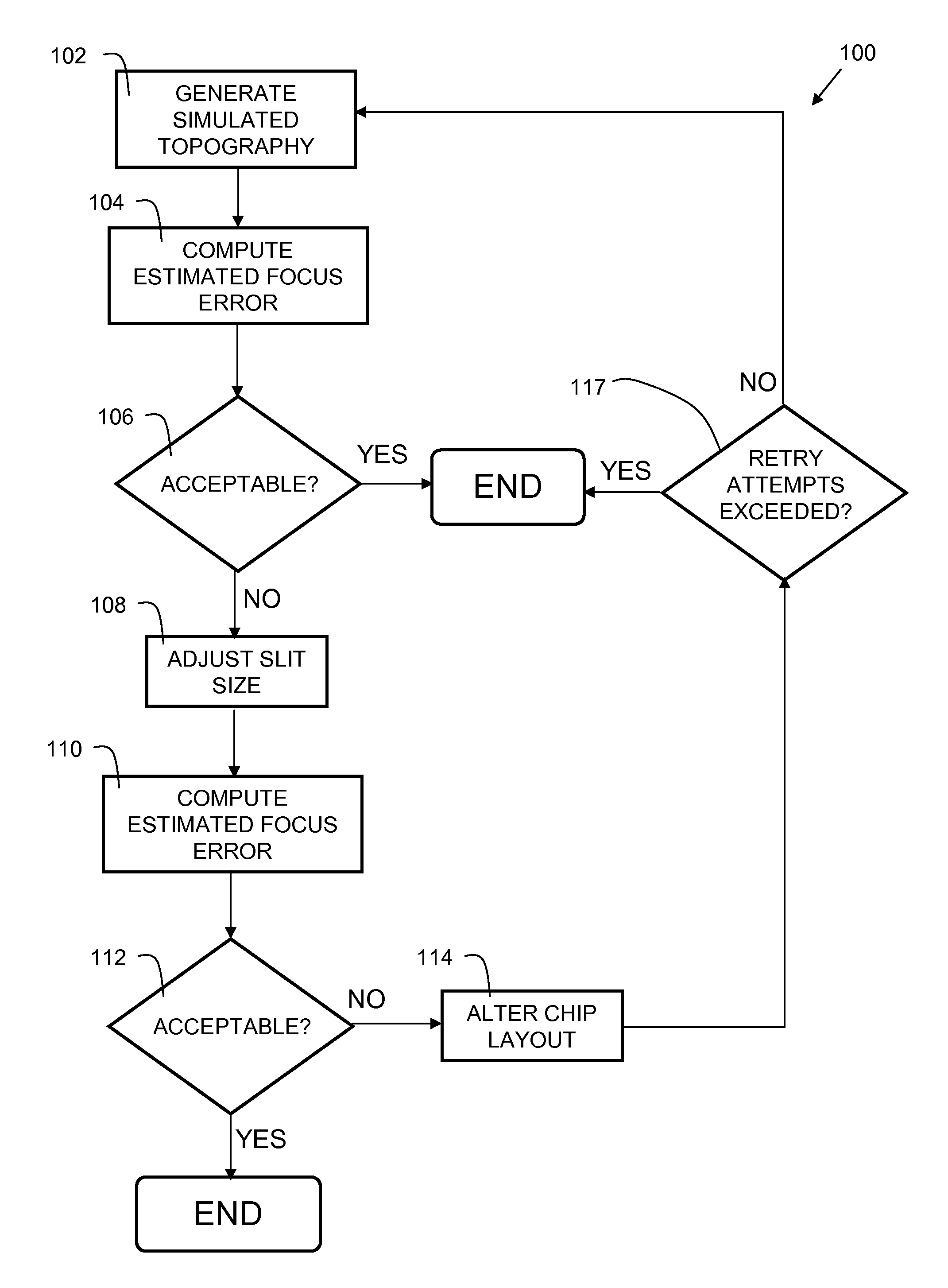
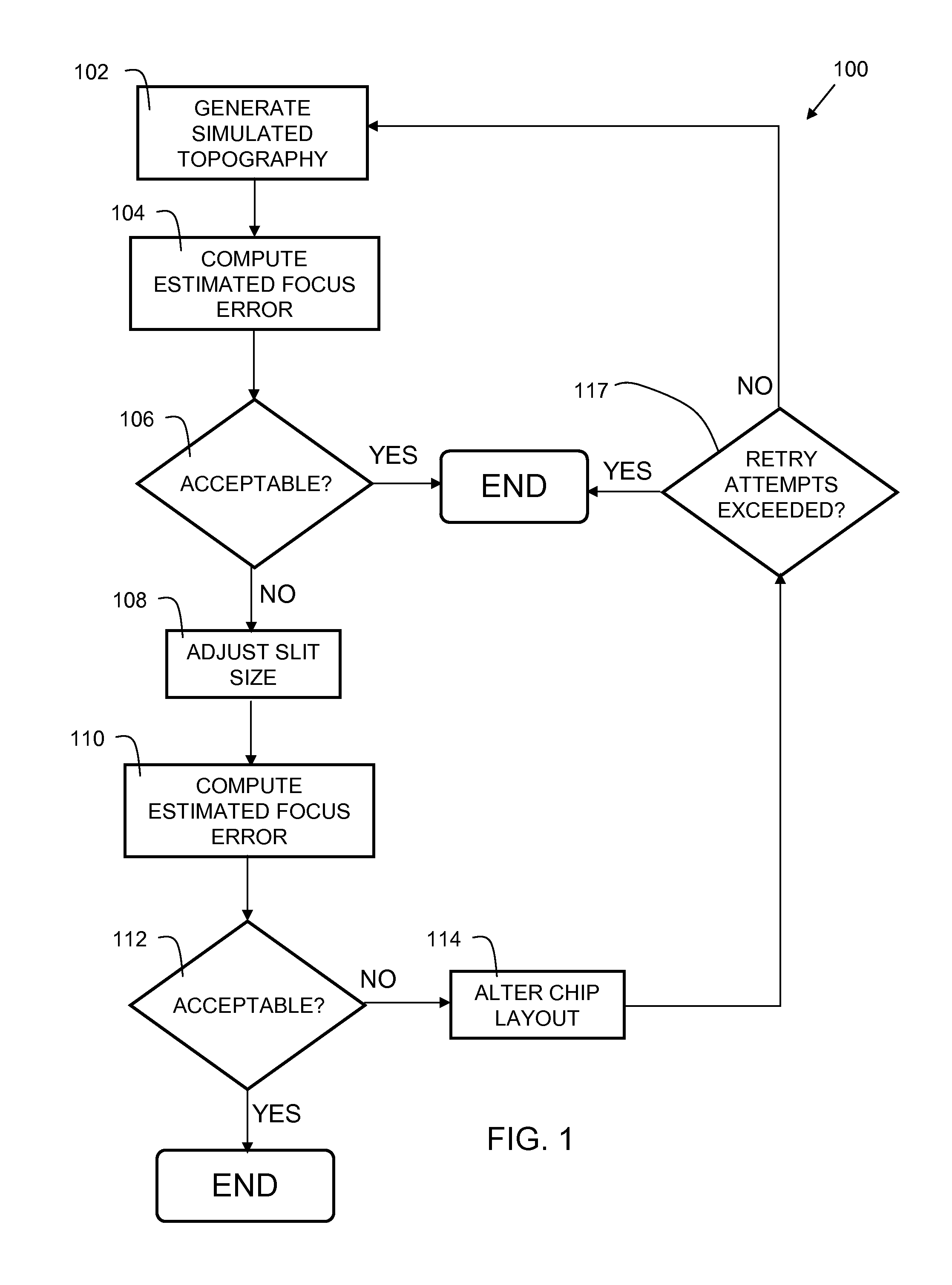
[0005]In one embodiment of the present invention, a method is provided for predicting lithography focus error for a chip. The method comprises computing a focal plane that best fits a subset of chip topography data. Then, a minimal local residual of the focal plane is computed. Next, a total focus error value is updated with the minimal local residual. Next, a new subset of chip topography data is acquired. These steps then repeat until each data point within the chip topography data is considered in at least one subset, resulting in the computation of a focus error value for the chip.

Problems solved by technology

These steps then repeat until each data point within the chip topography data is considered in at least one subset, resulting in the computation of a focus error value for the chip.

Method used


Image

  • Method and system to predict lithography focus error using simulated or measured topography
  • Method and system to predict lithography focus error using simulated or measured topography
  • Method and system to predict lithography focus error using simulated or measured topography

Examples


Embodiment Construction

[0014]Topography refers to the variation in height (Z) above the surface of a substrate. In semiconductor fabrication, typically a planarization step, such as a chemical mechanical polish (CMP) is performed to make the surface of the substrate smooth, such that a subsequent layer of the semiconductor can be formed. Typically, the first step in forming a layer of a multilayer integrated circuit (IC) is deposition of a mask layer, followed by a patterning step. Regions of the mask are cured via a lithographic process. Lithography tools focus an image onto the mask layer to cure a portion of the mask, while other parts of the mask remain uncured. The result is a pattern that is used in formation of subsequent layers used in the semiconductor fabrication process. Ideally, the planarization step makes the substrate completely smooth. However, in practice, there are variations in height (Z variations) due in part to the differing material characteristics of the various materials (e.g. pol...


PUM


Abstract

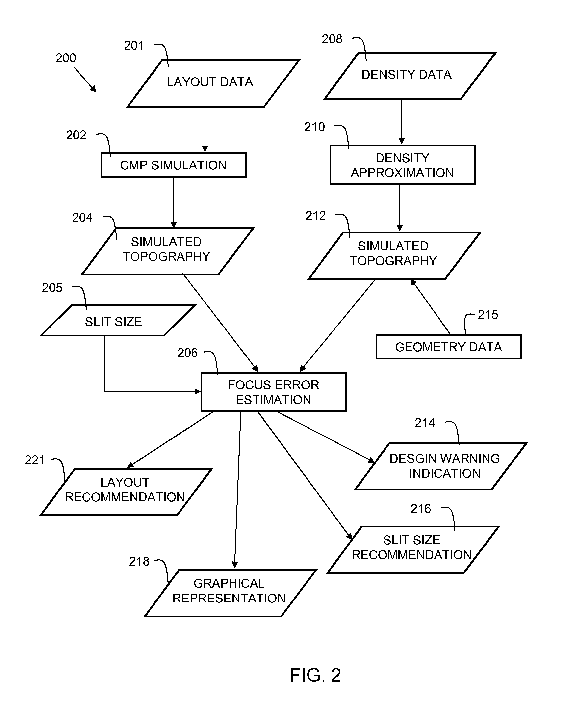
A method and system to predict lithography focus error using chip topography data is disclosed. The chip topography data may be measured or simulated topography data. A plane is best fitted to the topography data, and residuals are computed. The residuals are then used to make a prediction regarding the focus error. The density ratio of metal to dielectric may also be used as a factor in determining the predicted focus error.

Description

FIELD OF THE INVENTION[0001]The present invention relates generally to semiconductor fabrication, and more particularly, the present invention relates to lithographic processes used in semiconductor fabrication.BACKGROUND OF THE INVENTION[0002]Conventional optical projection lithography has been the standard silicon patterning technology for many years. It is an economical process due to its inherently high throughput, thereby providing a desirable low cost per part or die produced. A considerable infrastructure (including steppers, photomasks, resists, metrology, etc.) has been built up around this technology.[0003]In this process, a mask, or “reticle”, includes a device pattern formed of an opaque material, such as chrome, on a transparent or semitransparent substrate. The transmission of the opaque material may also vary, such as in the case of an attenuating phase shift mask. The device pattern of the reticle can be transferred to a photoresist film using imaging techniques well...

Claims


Application Information

Patent Timeline
Patent Type & Authority Applications(United States)
IPC IPC(8): G03B27/52
CPCG03F7/70066G03F7/705G03F7/70641G06F17/5009G03F7/7065G03F7/70525G06F17/5081G03F9/7026G06F30/20G06F30/398
Inventor SAPP, BRIAN CHRISTOPHERCHO, CHOONGYEUNCLEVENGER, LAWRENCE A.ECONOMIKOS, LAERTISLIEGL, BERNHARD R.PETRARCA, KEVIN S.QUON, ROGER ALLAN
Owner IBM CORP
Learn More