Packaging Photon Building Blocks Having Only Top Side Connections in a Molded Interconnect Structure
- Summary
- Abstract
- Description
- Claims
- Application Information
AI Technical Summary
Benefits of technology
Problems solved by technology
Method used
Image
Examples
Embodiment Construction
[0110]Reference will now be made in detail to some embodiments of the invention, examples of which are illustrated in the accompanying drawings.
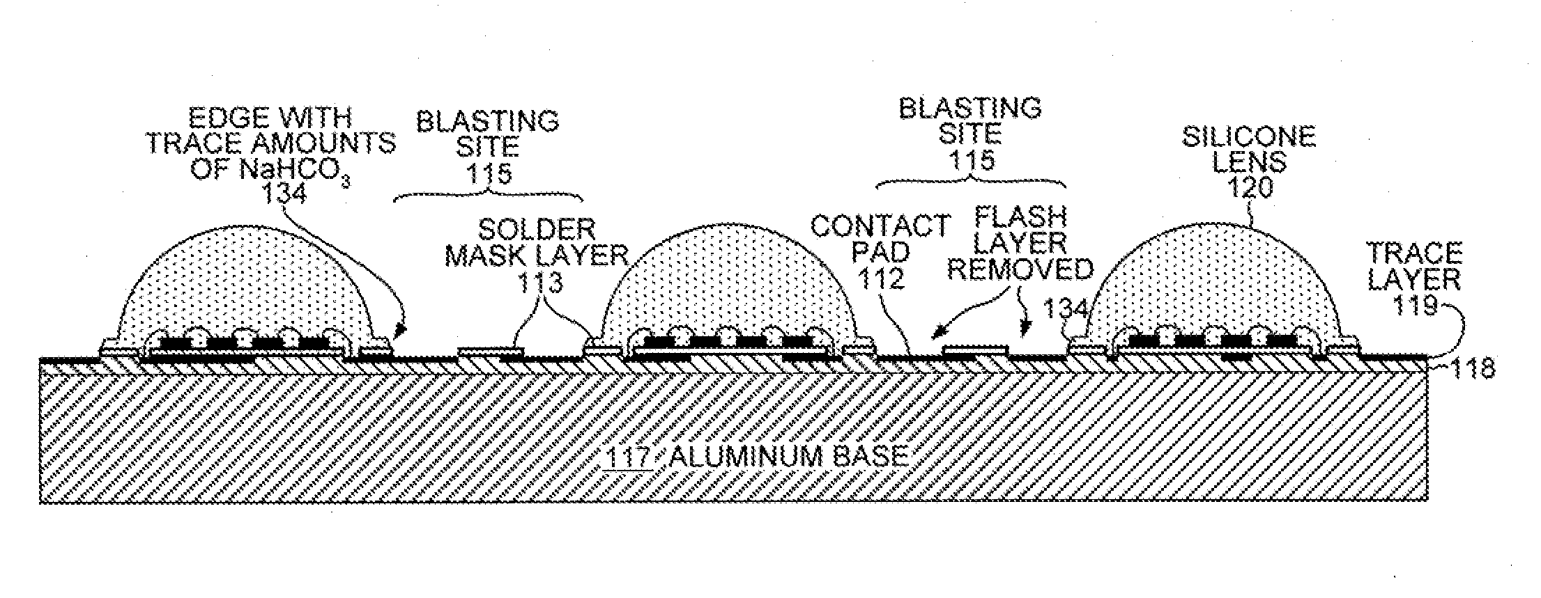
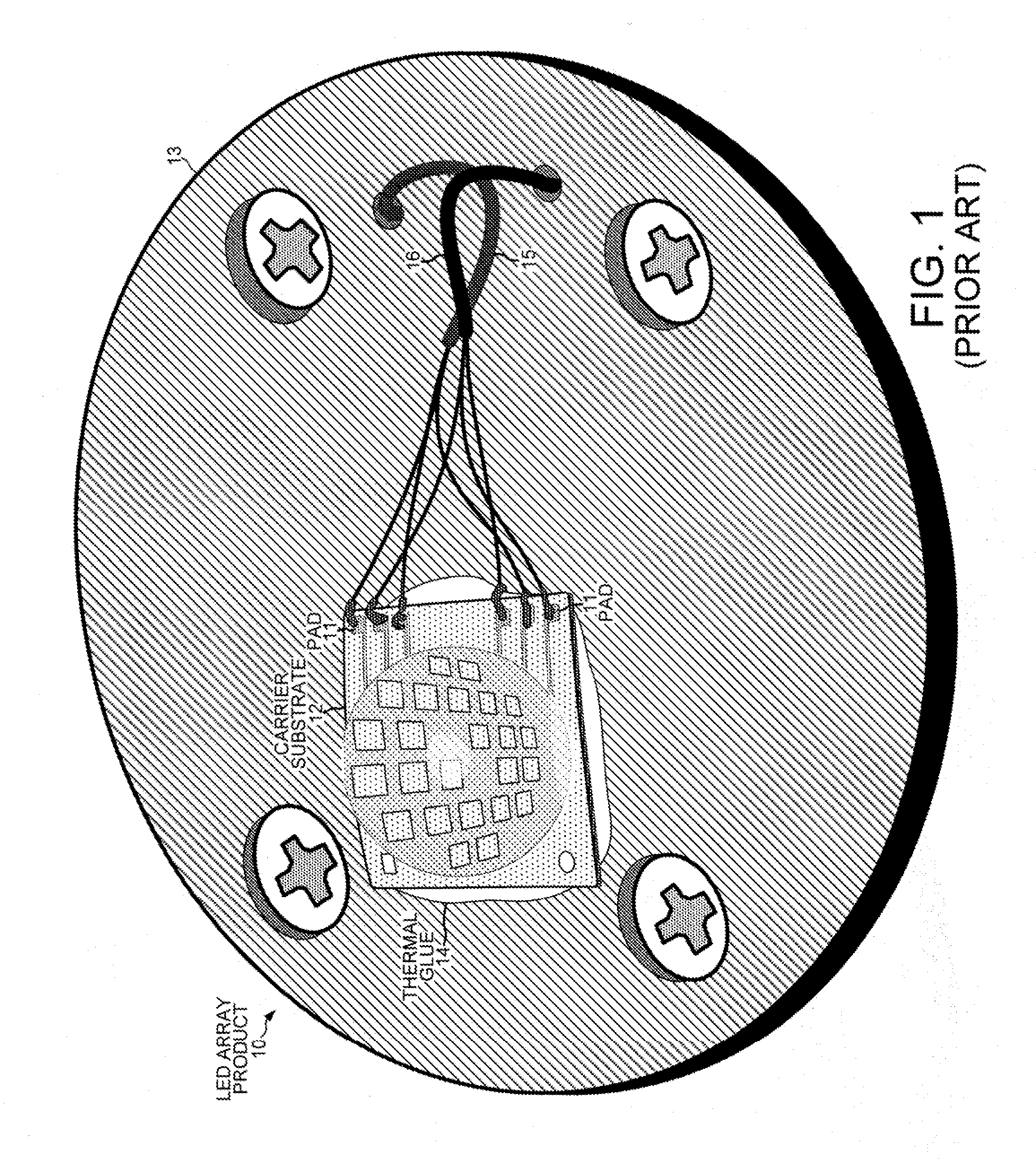
[0111]Systems and methods for manufacturing and processing LED devices using standard semiconductor packaging technologies and equipment are disclosed. The systems and methods enable LED package sizes to be shrunk to sizes that are smaller than can be made using conventional LED packaging technologies. In addition, a more efficient and less costly interface interconnect between an LED die / array and the packaging is disclosed.
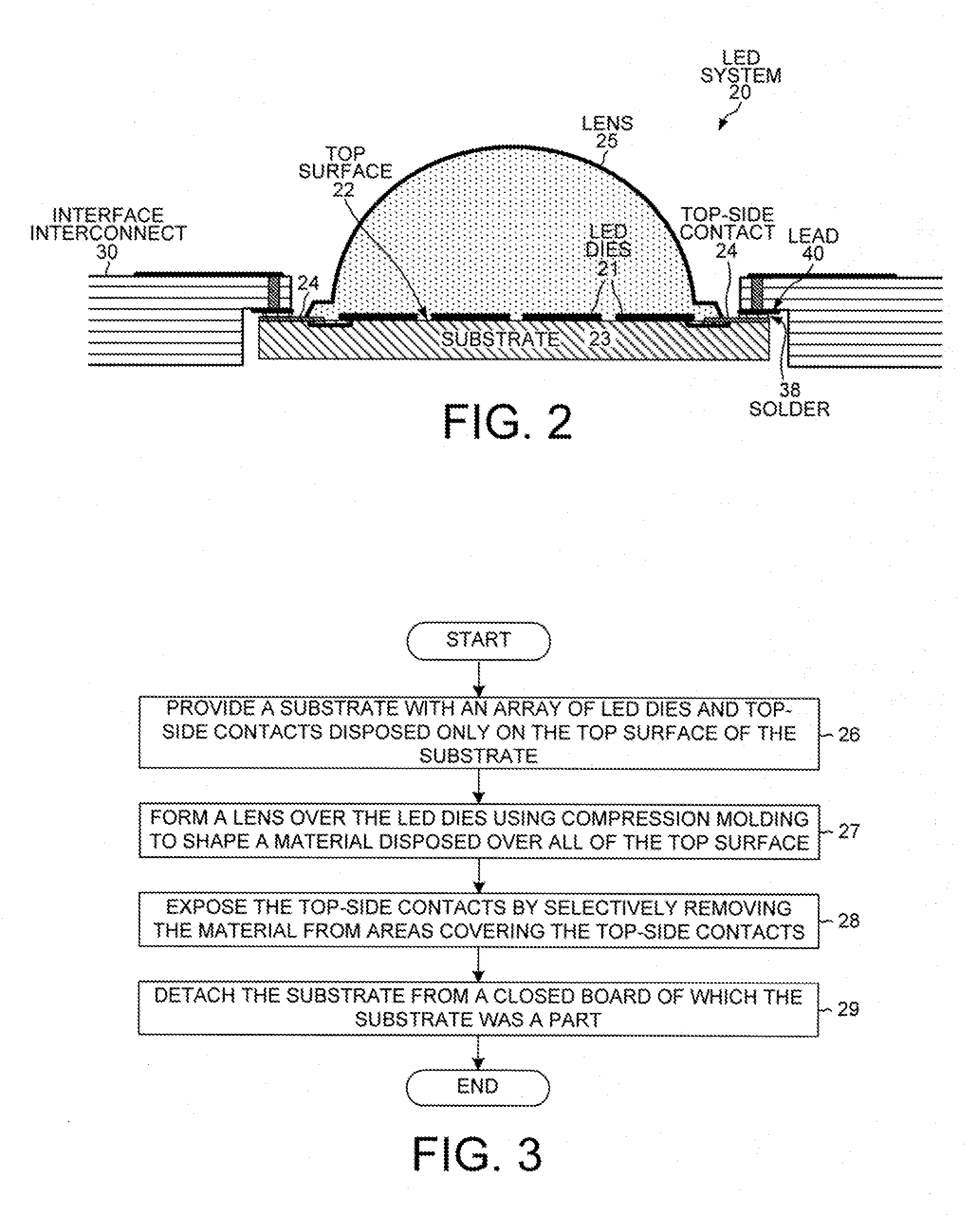
[0112]In one embodiment, an LED is fabricated by providing a substrate with an array of LED dies and top-side contacts. One or more lenses are formed over the array of LED dies using compression molding such that one lens is formed over at least one of the LED dies. The top-side contacts are exposed by selectively removing material from areas covering the top-side contacts. Fabricating LED lens in this manner enables low...
PUM
 Abstract
Description
Claims
Application Information
 - R&D
- Intellectual Property
- Life Sciences
- Materials
- Tech Scout
- Unparalleled Data Quality
- Higher Quality Content
- 60% Fewer Hallucinations
Browse by: Latest US Patents, China's latest patents, Technical Efficacy Thesaurus, Application Domain, Technology Topic, Popular Technical Reports.
© 2025 PatSnap. All rights reserved.Legal|Privacy policy|Modern Slavery Act Transparency Statement|Sitemap|About US| Contact US: help@patsnap.com


