Grid for radiography, radiation image detector, radiation imaging system, and method for manufacturing grid
a technology of radiography and grids, applied in the field of grids for radiography, radiation image detectors, radiation imaging systems, and manufacturing grids, can solve the problems of high cost of dry etching methods, low throughput, and limited application, so as to prevent the diffusion of gold, reduce the cost of exposure, and reduce the effect of aging
- Summary
- Abstract
- Description
- Claims
- Application Information
AI Technical Summary
Benefits of technology
Problems solved by technology
Method used
Image
Examples
first embodiment
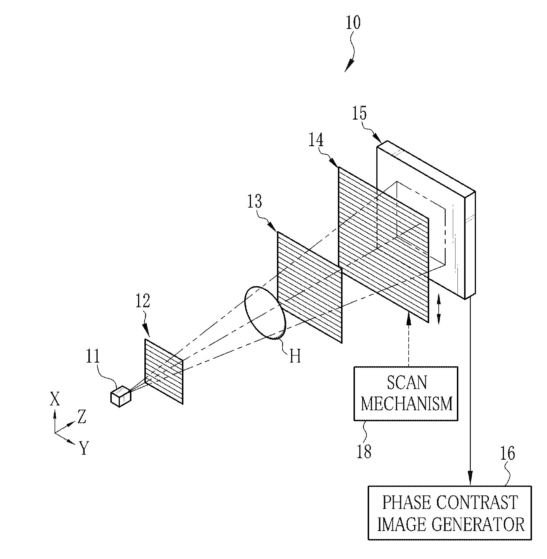
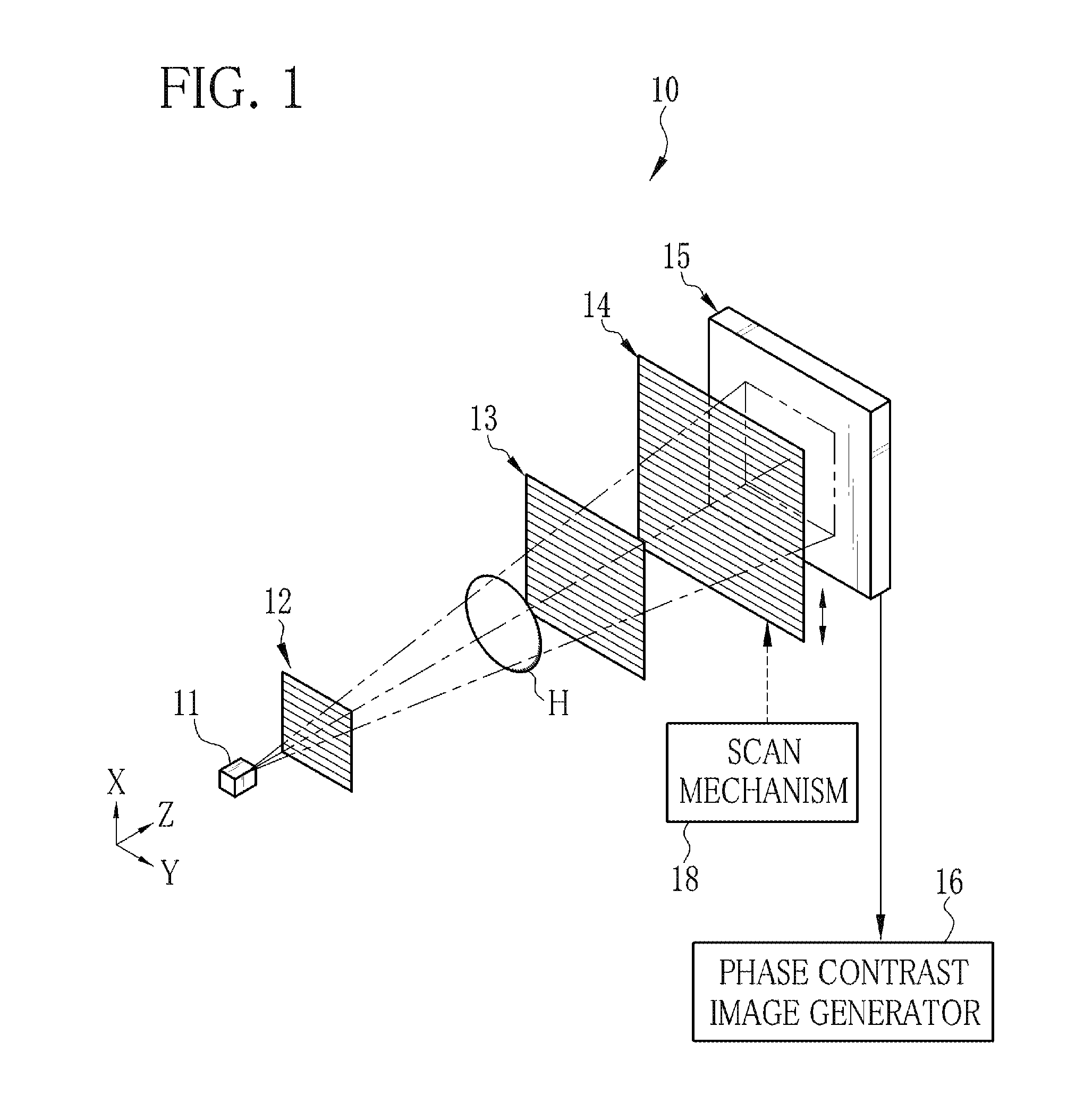
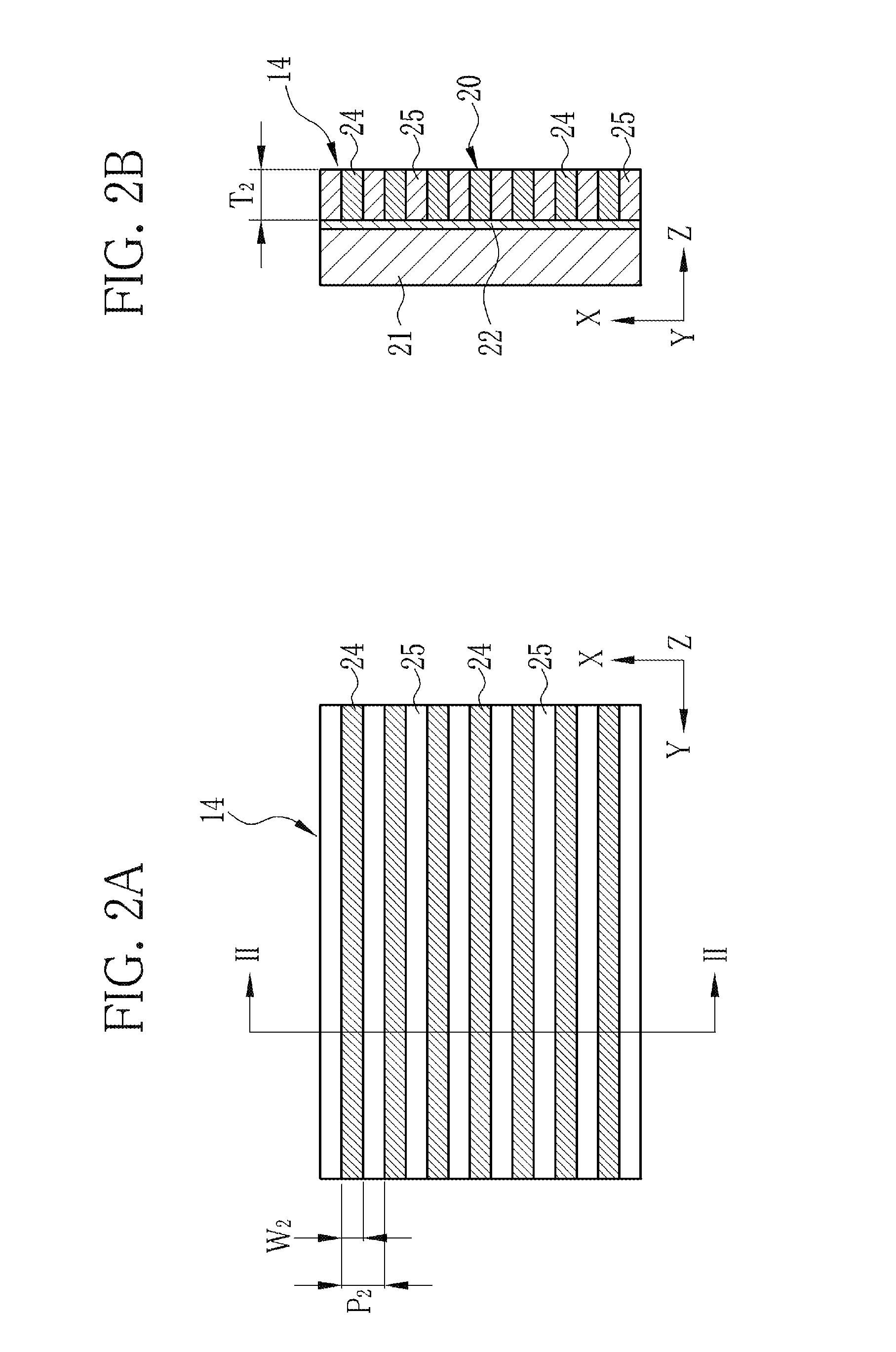
[0042]As shown in FIG. 1, an X-ray imaging system 10 is constituted of an X-ray source 11, a source grid 12, a first grid 13, a second grid 14, and an X-ray image detector 15, which are disposed in a Z direction being an X-ray propagation direction. The X-ray source 11 has, for example, a rotating anode type X-ray tube and a collimator for limiting an irradiation field of X-rays, and applies a cone beam of X-rays to a sample H. The X-ray image detector 15 is a flat panel detector (FPD) composed of semiconductor circuitry, for example, and is disposed behind the second grid 14. To the X-ray image detector 15, a phase contrast image generator 16 is connected to produce a phase contrast image from image data detected by the X-ray image detector 15.
[0043]The source grid 12, the first grid 13, and the second grid 14 being X-ray absorption grids are opposite to the X-ray source 11 in the Z direction. The sample H is disposed between the source grid 12 and the first grid 13. The distance b...
second embodiment
[0071]In a second embodiment, the nonlinear single crystal substrate doped with a phosphor is integrated into the X-ray image detector, and is used as the second grid and the scintillator. As shown in FIG. 12, before or after the X-ray absorbing material 48 is charged into the grooves 40e of the nonlinear single crystal substrate 40, the reversed portions 40c may be doped with the phosphor. In another case, the nonlinear single crystal substrate doped with the phosphor may be manufactured, and then the X-ray absorbing material 48 may be charged into the grooves 40e. After that, the seed layer 22 is removed to take out the nonlinear single crystal substrate 40. As shown in FIG. 13, this nonlinear single crystal substrate 40 emits light upon application of the X-rays. Then, as shown in FIG. 14, the nonlinear single crystal substrate 40 is contained in an X-ray image detector 60, so the nonlinear single crystal substrate 40 functions as the second grid and the scintillator. In the case...
third embodiment
[0073]In the above embodiments, the polarization inversion is performed straight along a thickness direction of the nonlinear single crystal substrate 40. However, as shown in FIG. 16, second periodic electrodes 70 with different periodicity from that of the periodic electrodes 41 of the first surface 40a maybe formed in the second surface 40b of the nonlinear single crystal substrate 40. After that, voltage is applied from the high voltage source 46 to the second periodic electrodes 70, so the polarization inversion occurs between the periodic electrode 41 and the second periodic electrode 70. According to this embodiment, as shown in a grid 75 of FIG. 17, the X-ray absorbing portions 24 and the X-ray transparent portions 25 can be inclined in a grid surface, such that the X-rays emitted from behind the grid 75 and passed through the X-ray transparent portions 25 converge to the X-ray focus 11a being an X-ray generation point of the X-ray source 11. Thereby, it is possible to reduc...
PUM
 Abstract
Description
Claims
Application Information
 - R&D
- Intellectual Property
- Life Sciences
- Materials
- Tech Scout
- Unparalleled Data Quality
- Higher Quality Content
- 60% Fewer Hallucinations
Browse by: Latest US Patents, China's latest patents, Technical Efficacy Thesaurus, Application Domain, Technology Topic, Popular Technical Reports.
© 2025 PatSnap. All rights reserved.Legal|Privacy policy|Modern Slavery Act Transparency Statement|Sitemap|About US| Contact US: help@patsnap.com


