
Vertical channel transistor array and manufacturing method thereof

a technology of vertical channel transistors and manufacturing methods, applied in the direction of semiconductor devices, basic electric elements, electrical apparatus, etc., can solve the problems of increasing the complexity of the semiconductor manufacturing process, affecting the electrical performance of the semiconductor, and the current is likely to decrease, so as to reduce the size and improve the device performance

Active Publication Date: 2012-07-19
POWERCHIP SEMICON MFG CORP
View PDF2 Cites 16 Cited by
  • Summary
  • Abstract
  • Description
  • Claims
  • Application Information

AI Technical Summary

Benefits of technology

[0008]In view of the above, the invention is directed to a vertical channel transistor array and a manufacturing method thereof for reducing size and improving performance of devices.
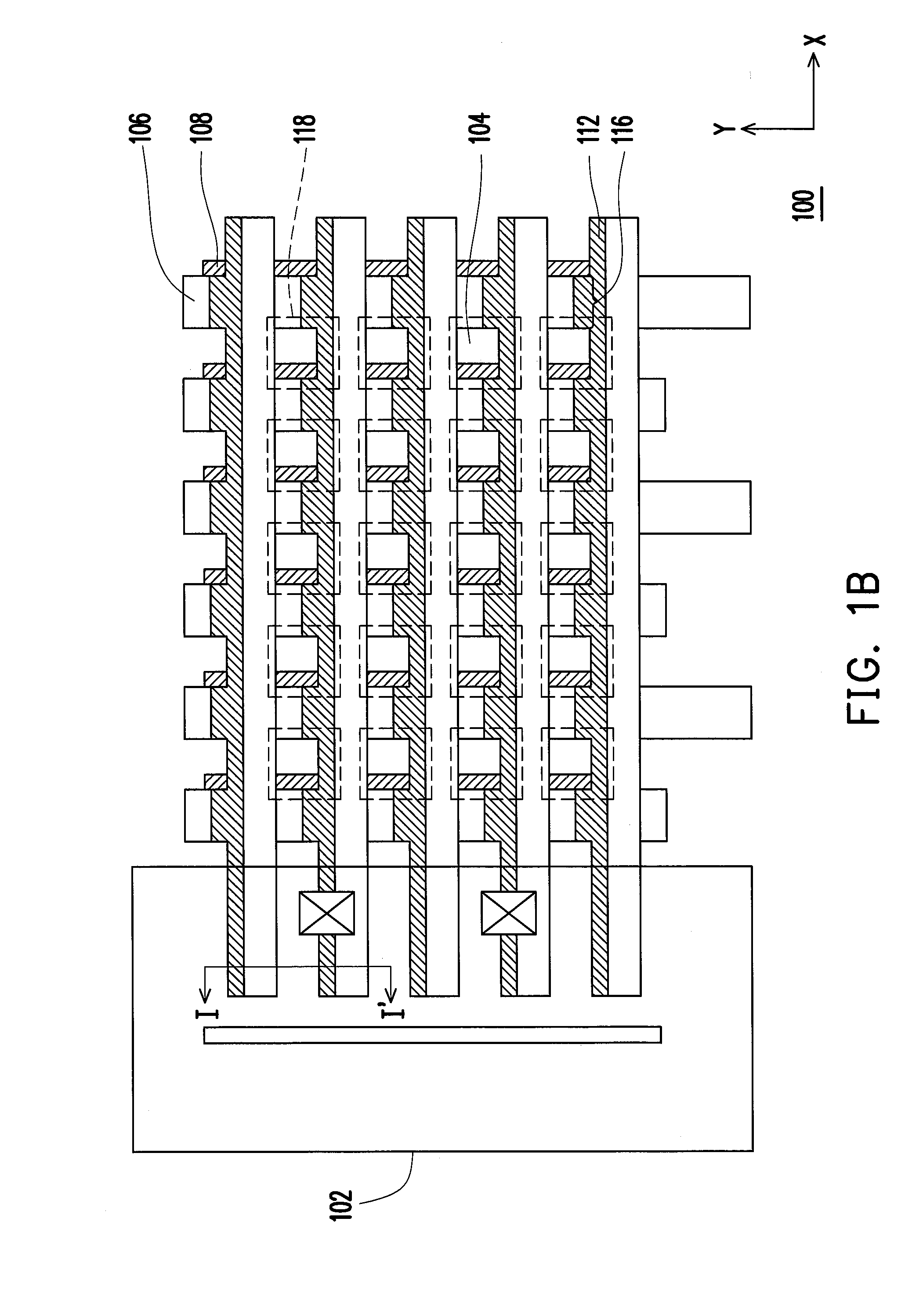
[0040]In the vertical channel transistor array of the invention, only one of the embedded word lines is disposed on the semiconductor pillars in one row, and therefore device dimension can be reduced. Besides, each of the embedded word lines selectively has a plurality of extending portions. Each of the extending portions is disposed between two adjacent semiconductor pillars in the same row, so as to increase the channel area of the device and effectively prevent short channel effects. Thereby, device performance is improved.
[0041]On the other hand, in the vertical channel transistor array of the invention, the embedded word lines and the back gate are respectively disposed at two opposite sides of the semiconductor pillars. The back gate can protect the semiconductor pillars from being etched during the etching process. Meanwhile, during operation of the semiconductor device of the invention, the adjacent embedded word lines are not interfered with each other, so as to improve device performance.

Problems solved by technology

Thereby, however, a significant short channel effect occurs in the transistors, and an On current is likely to decrease.
As such, complexity of the semiconductor manufacturing process is raised, and electrical performance of the semiconductor is likely to be affected.

Method used


Image

  • Vertical channel transistor array and manufacturing method thereof
  • Vertical channel transistor array and manufacturing method thereof
  • Vertical channel transistor array and manufacturing method thereof

Examples


first embodiment

[0083]FIG. 2A(1)˜FIG. 2M(1) are cross-sectional views illustrating a manufacturing process depicted in FIG. 1C taken along the line A-A′. FIG. 2A(2)˜FIG. 2M(2) are cross-sectional views illustrating a manufacturing process depicted in FIG. 1C taken along the line B-B′. FIG. 2A(3)˜FIG. 2F(3) are cross-sectional views illustrating a manufacturing process depicted in FIG. 1C taken along the line C-C′.

[0084]With reference to FIG. 2A(1) to FIG. 2A(3), a semiconductor substrate 100 is provided. The semiconductor substrate 100, for example, is a silicon substrate.

[0085]A mask layer 126 is formed on the substrate 100. A material of the mask layer 126 is, for example, silicon nitride. A method of forming the mask layer 126 is, for example, chemical vapor deposition. The mask layer 126 and the semiconductor substrate 100 are patterned to form a plurality of trenches 128. The trenches 128 are disposed in parallel in the semiconductor substrate 100 and extended in a column direction (Y directio...

second embodiment

[0106]FIG. 4A(1)˜FIG. 4G(1) are cross-sectional views illustrating a manufacturing process depicted in FIG. 1G taken along a line A-A′. FIG. 4A(2)˜FIG. 4G(2) are cross-sectional views illustrating a manufacturing process depicted in FIG. 1G taken along a line B-B′. FIG. 4A(1) to FIG. 4G(1) follow FIG. 2F(1); FIG. 4A(2) to FIG. 4G(2) follow FIG. 2F(2).

[0107]With reference to FIG. 4A(1) to FIG. 4A(2), a sacrificial layer 148a is formed on the semiconductor substrate 100, and the trenches 128 are filled with the sacrificial layer 148a. A material of the sacrificial layer 148a includes SOD materials, such as HSQ, MSQ, or organic materials. Besides, the sacrificial layer 148a is formed by performing a spin-coating process to form a SOD material layer and then performing a baking process on the SOD material layer, for example. A planarization process (e.g. a chemical mechanical polishing process or an etch-back process) is carried out to remove a portion of the SOD material layer and expo...

third embodiment

[0116]FIG. 5A(1)˜FIG. 5H(1) are cross-sectional views illustrating a manufacturing process depicted in FIG. 1G taken along the line A-A′. FIG. 5A(2)˜FIG. 5H(2) are cross-sectional views illustrating a manufacturing process depicted in FIG. 1G taken along the line B-B′. FIG. 5A(1) to FIG. 5H (1) follow FIG. 2F(1); FIG. 5A(2) to FIG. 5H(2) follow FIG. 2F(2).

[0117]With reference to FIG. 5A(1) to FIG. 5A(2), an inter-layer insulating layer 148 completely filling the trenches 128 is formed on the semiconductor substrate 100. A material of the inter-layer insulating layer 148 includes SOD materials, such as HSQ, MSQ, or organic materials. Besides, the inter-layer insulating layer 148 is formed by performing a spin-coating process to form a SOD material layer and then performing a baking process on the SOD material layer, for example. A planarization process (e.g. a chemical mechanical polishing process or an etch-back process) is carried out to remove a portion of the SOD material layer a...


PUM


Abstract

A vertical channel transistor array includes a plurality of embedded bit lines, a plurality of bit line contacts, a plurality of embedded word lines, and a current leakage isolation structure. An active area of a vertical channel transistor is defined by the semiconductor pillars. The embedded bit lines are disposed in parallel in a semiconductor substrate and extended in a column direction. Each of the bit line contacts is respectively disposed at a side of one of the embedded bit lines. The embedded word lines are disposed in parallel above the embedded bit lines and extended in a row direction. Besides, the embedded word lines and the semiconductor pillars in the same row are connected but spaced by a gate dielectric layer. The current leakage isolation structure is disposed at ends of the embedded bit lines to prevent current leakage between the adjacent bit line contacts.

Description

BACKGROUND OF THE INVENTION[0001]1. Field of the Invention[0002]The invention relates to a semiconductor device and a manufacturing method thereof. More particularly, the invention relates to a vertical channel transistor array and a manufacturing method thereof.[0003]2. Description of Related Art[0004]With the development of powerful microprocessors, software is more capable of programming and calculating an increasing amount of data. Therefore, the fabrication of memories has become essential in the semiconductor industry. A dynamic random access memory (DRAM) is a volatile memory (VM) and is constituted by a plurality of memory cells. Each of the memory cells in the VM is mainly composed of a transistor and a capacitor, and all memory cells are electrically connected to one another through word lines (WL) and bit lines (BL).[0005]As science advances day by day, the length of the channel region of each transistor in the DRAM is gradually decreased together with the reduction of th...

Claims


Application Information

Patent Timeline
IPC IPC(8): H01L29/78H01L21/336
CPCH01L27/10823H01L27/10876H01L27/10844H01L27/10891H01L27/10885H10B12/34H10B12/053H10B12/482H10B12/488H10B12/01
Inventor NAGAI, YUKIHIRO
Owner POWERCHIP SEMICON MFG CORP
Learn More