Method for manufacturing piezoelectric element
a piezoelectric element and manufacturing method technology, applied in mechanical vibration separation, mechanical apparatus, operating means/releasing devices of valves, etc., can solve the problems of easy generation of differences in crystal orientation degree, crystal formation, intrinsic polarization state, and difficult to obtain a flat fired piezoelectric body (piezoelectric element), etc., to achieve excellent flatness, less damage, and less warpage
- Summary
- Abstract
- Description
- Claims
- Application Information
AI Technical Summary
Benefits of technology
Problems solved by technology
Method used
Image
Examples
example 1
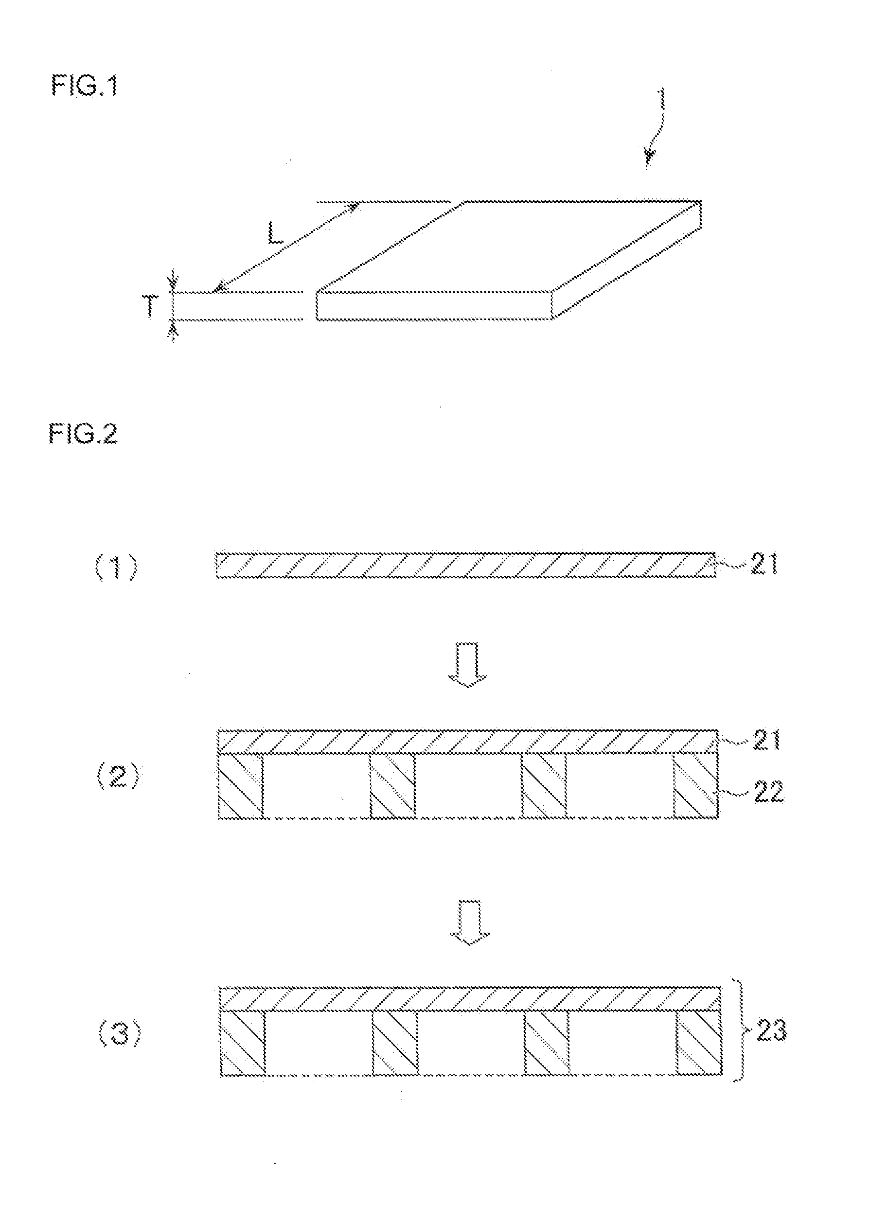
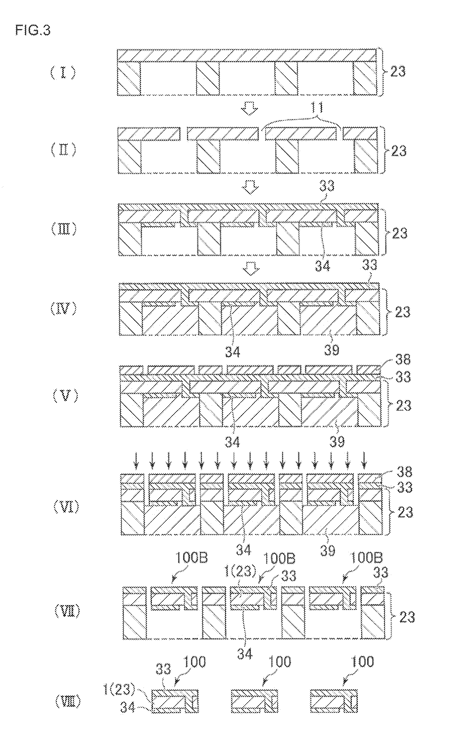
[0054]A piezoelectric element precursor fixed by three bonding portions as one piezoelectric element precursor in FIG. 7 was manufactured according to a method for manufacturing a piezoelectric element of the present invention. Specifically, in the first place, there was obtained a fired piezoelectric body having a rectangular shape of 2 mm×4 mm and a thickness of 15 μm. The thickness of the fired piezoelectric body was 15 μm, and the surface roughness Ra was 0.19 μm on one surface of the fired piezoelectric body while it was 0.1 μm on the other surface. As the piezoelectric material, there was used 0.17Pb(Mg1 / 3Nb2 / 3)O3-0.03Pb(Ni1 / 3Nb2 / 3)O3-0.43PbTi O3-0.37PbZrO3. The same piezoelectric material was used for the reinforcers (corresponding to the reinforcers 22 of the step (2) of FIG. 2) for firing, and the reinforcers were formed by screen printing to have a thickness of 30 μm. The firing was performed at 1200° C. for two hours. Gold (Au) was used for the electrode, which was formed...
example 2
[0056]There was manufactured a piezoelectric element precursor fixed by two bonding portions like one piezoelectric element precursor in FIG. 4, and polarization was performed in the same manner as in Example 1 except for the aforementioned point to obtain a piezoelectric element. The undulation amount for 10 elements was measured, and it was 0.5 to 30 μm. Then, a drive durability test was performed by a rectangular wave of 10V at 5 kHz for one hour to confirm that no problem was caused.
PUM
| Property | Measurement | Unit |
|---|---|---|
| temperature | aaaaa | aaaaa |
| thickness | aaaaa | aaaaa |
| thickness | aaaaa | aaaaa |
Abstract
Description
Claims
Application Information
 - Generate Ideas
- Intellectual Property
- Life Sciences
- Materials
- Tech Scout
- Unparalleled Data Quality
- Higher Quality Content
- 60% Fewer Hallucinations
Browse by: Latest US Patents, China's latest patents, Technical Efficacy Thesaurus, Application Domain, Technology Topic, Popular Technical Reports.
© 2025 PatSnap. All rights reserved.Legal|Privacy policy|Modern Slavery Act Transparency Statement|Sitemap|About US| Contact US: help@patsnap.com


