Semiconductor laser device and method for producing the same

a laser device and semiconductor technology, applied in the direction of lasers, semiconductor lasers, solid-state devices, etc., can solve the problems of degrading the high-frequency response characteristics and the difficulty of obtaining the high-speed operation of the semiconductor laser device, so as to improve the parasitic capacitance of the device, increase the capacity, and reduce the parasitic capacitance

Inactive Publication Date: 2012-04-19
SUMITOMO ELECTRIC IND LTD
View PDF3 Cites 4 Cited by
  • Summary
  • Abstract
  • Description
  • Claims
  • Application Information

AI Technical Summary

Benefits of technology

[0005]With the increased capacity of recent optical fiber communication systems, semiconductor laser devices with a high-speed operation of 10 gigabits per second (Gbps) or more has been desired. Ridge-type semiconductor laser devices can be operated at a high speed because the parasitic capacitance of the devices can be reduced.
[0010]The semiconductor laser device according to the embodiment includes a first semiconductor stack portion that includes a grating layer and an active layer provided on the grating layer, the grating layer having a first region and second region; a diffraction grating provided in the first region of the grating layer; and a semiconductor ridge structure portion provided on the first semiconductor stack portion. Furthermore, a pair of first trenches is provided in the first semiconductor stack portion along both side faces of the semiconductor ridge structure portion. The first region of the grating layer is located between the pair of first trenches. In addition, the pair of first trenches extends so as to penetrate through the grating layer. Furthermore, an end of the first region of the grating layer reaches the first trench. With this configuration, it is possible to effectively prevent a current from flowing through peripheral regions of the grating layer in a bypass manner. Thus, according to this semiconductor laser device, the current mainly flows through the diffraction grating, and thus good high-frequency response characteristics can be realized.
[0018]In the method for producing a semiconductor laser device, a diffraction grating is formed by etching a grating layer through a mask that has been patterned by an electron beam (EB) lithography method. The EB lithography method requires a long time for patterning, as compared with other methods such as an interference lithography method. Therefore, in order to reduce the time necessary for forming the diffraction grating, a width of the diffraction grating is decreased, and a pattern for forming the diffraction grating is formed in a region having a width smaller than a width of a semiconductor substrate in a second direction that intersects with the first direction. Thus, the electron beam (EB) drawing time can be reduced. In addition, a pair of first trenches is formed in a first region of the grating layer where the diffraction grating is formed. Accordingly, a current can be concentrated in a portion of the grating layer located between the pair of first trenches. Therefore, even when a diffraction grating is formed not over the entire surface of the device, but on a portion of the surface thereof so as to have a small width, it is possible to prevent a current from flowing through the peripheral regions of the grating layer in a bypass manner. Therefore, a high speed semiconductor laser device with good high-frequency response characteristics can be obtained.

Problems solved by technology

However, it is difficult to obtain the high-speed operation for the semiconductor laser device with a diffraction grating arranged between a semiconductor substrate and an active layer, especially when the width of the diffraction grating is limited.
These may result in degrading the high-frequency response characteristics.

Method used


Image

  • Semiconductor laser device and method for producing the same
  • Semiconductor laser device and method for producing the same
  • Semiconductor laser device and method for producing the same

Examples


second embodiment

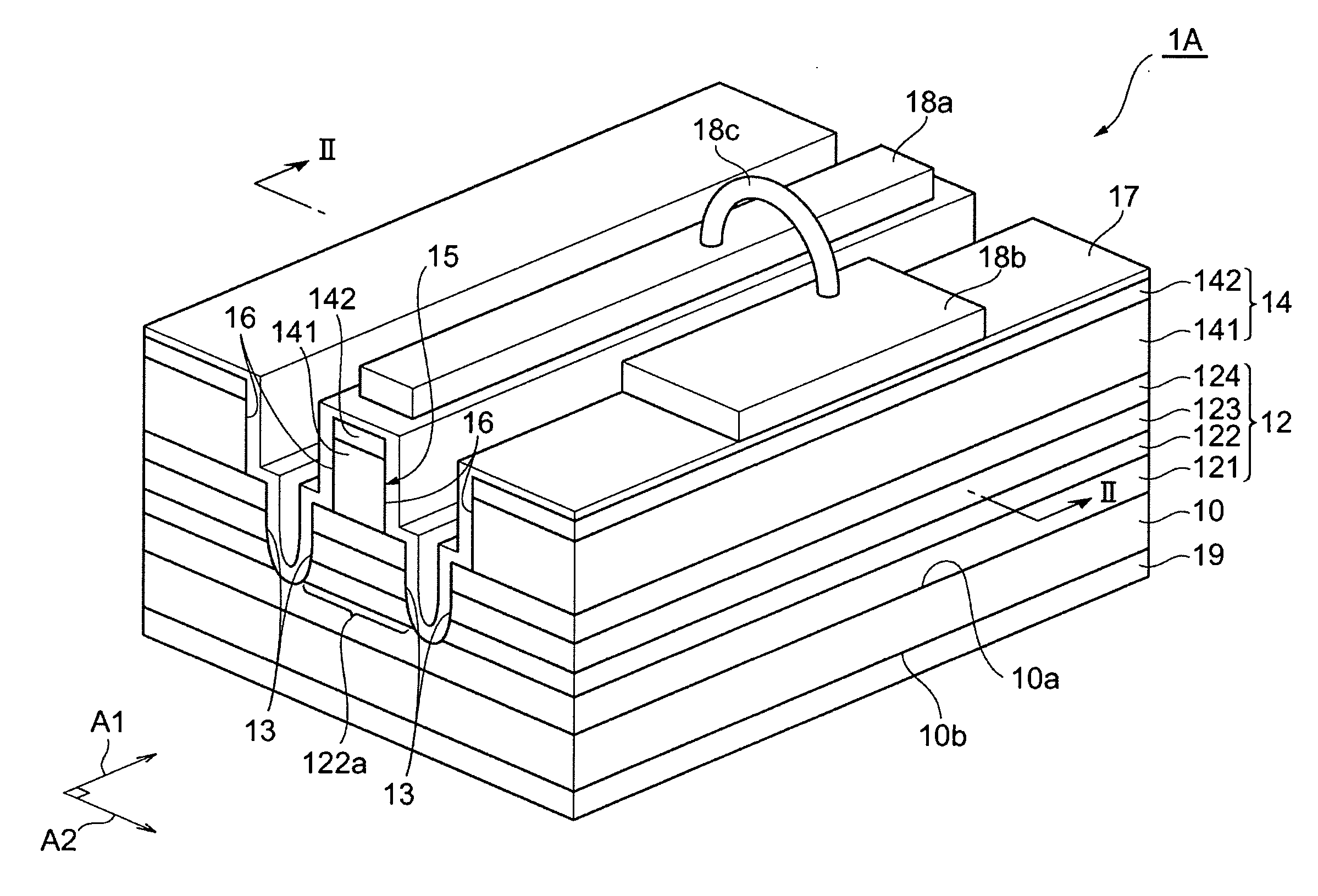
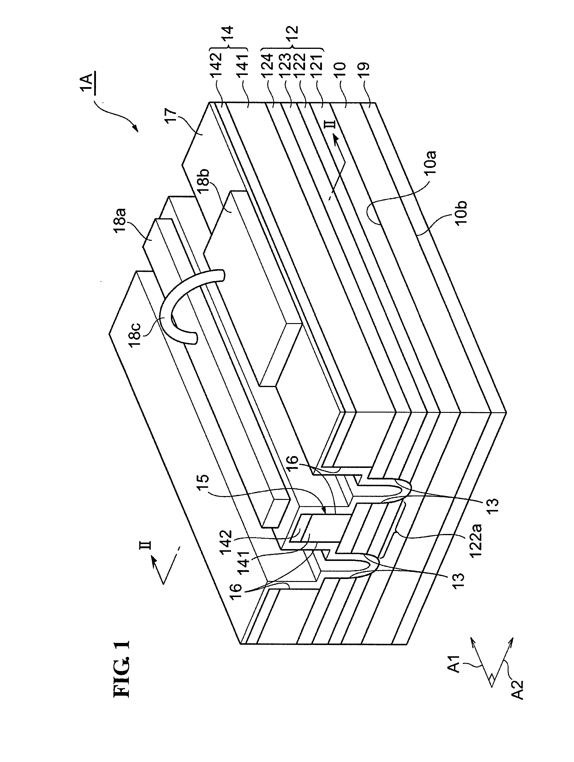
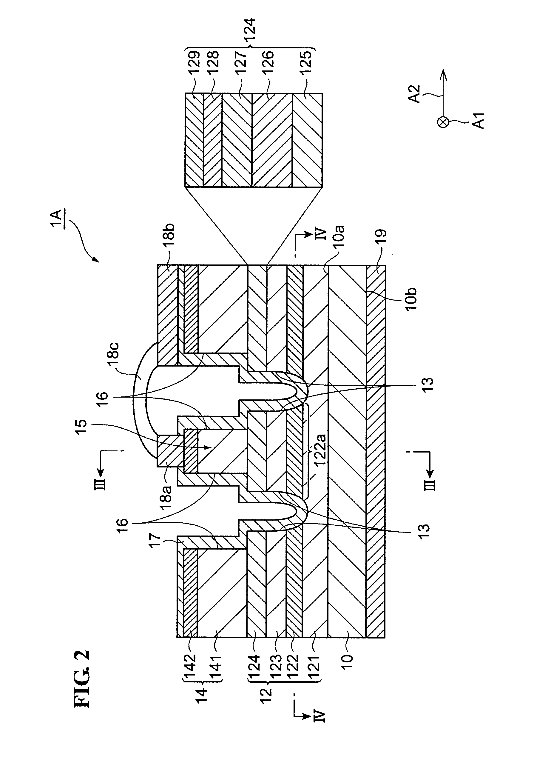
[0062]FIG. 8 is a cross-sectional view showing a configuration of a semiconductor laser device according to a second embodiment of the present invention. FIG. 9 is a cross-sectional view of the semiconductor laser device taken along line IX-IX of FIG. 8. A difference between a semiconductor laser device 1B of this embodiment and the semiconductor laser device 1A of the first embodiment will now be described.

[0063]The semiconductor laser device 1B of this embodiment differs from the semiconductor laser device 1A of the first embodiment in the configuration of a pair of first trenches 13. Specifically, the semiconductor laser device 1B includes a pair of first trenches 21 instead of the pair of first trenches 13 in the first embodiment. The pair of first trenches 21 is provided in order to block a current that bypasses a region where a diffraction grating 122a is formed. More specifically, the pair of first trenches 21 is formed along both side faces of a semiconductor ridge structure...


PUM


Abstract

A semiconductor laser device includes a first semiconductor stack portion that includes a grating layer and an active layer provided on the grating layer. The grating layer has a first region and second region; a diffraction grating provided in the first region; a semiconductor ridge structure portion provided on the first semiconductor stack portion and extending in a first direction; and a pair of first trenches provided along both side faces of the semiconductor ridge structure portion with the first region of the grating layer being located between the trenches. The first trenches penetrate through the grating layer. The first region of the grating layer has an end extending in a second direction intersecting with the first direction. The end of the first region of the grating layer reaches a trench.

Description

BACKGROUND OF THE INVENTION[0001]1. Field of the Invention[0002]The present invention relates to a semiconductor laser device and a method for producing the same.[0003]2. Description of the Related Art[0004]T. Takiguchi et al., “1.3 μm Uncooled AlGaInAs-MQW DFB laser with λ / 4-shifted Grating” Proceedings, Optical Fiber Communication Conference and Exhibit 2002, ThF3, pp. 417-418 (Non-Patent Reference 1) describes a ridge-type semiconductor laser device having a diffraction grating. In this semiconductor laser device described in this reference, the diffraction grating is formed inside a ridge on the upper side of an active layer.SUMMARY OF THE INVENTION[0005]With the increased capacity of recent optical fiber communication systems, semiconductor laser devices with a high-speed operation of 10 gigabits per second (Gbps) or more has been desired. Ridge-type semiconductor laser devices can be operated at a high speed because the parasitic capacitance of the devices can be reduced.[0006...

Claims


Application Information

Patent Timeline
IPC IPC(8): H01S5/026H01L33/58H01S5/12
CPCH01S5/06226H01S2301/176H01S5/2202H01S5/12H01L2224/48091H01L2224/48227H01L2924/00014
Inventor ONISHI, YUTAKA
Owner SUMITOMO ELECTRIC IND LTD
Why Eureka
Try Eureka