Photovoltaic cell with buffer zone
a photovoltaic cell and buffer zone technology, applied in the direction of basic electric elements, electrical apparatus, semiconductor devices, etc., can solve the problems of contributing any substantial series resistance loss in the photovoltaic cell, and achieve the effects of reducing the risk of auto-doping, and reducing the risk of oxidative damag
- Summary
- Abstract
- Description
- Claims
- Application Information
AI Technical Summary
Benefits of technology
Problems solved by technology
Method used
Image

Examples
Embodiment Construction
[0019]The various aspects of the subject innovation are now described with reference to the annexed drawings, wherein like numerals refer to like or corresponding elements throughout. It should be understood, however, that the drawings and detailed description relating thereto are not intended to limit the claimed subject matter to the particular form disclosed. Rather, the intention is to cover all modifications, equivalents, and alternatives falling within the spirit and scope of the claimed subject matter.
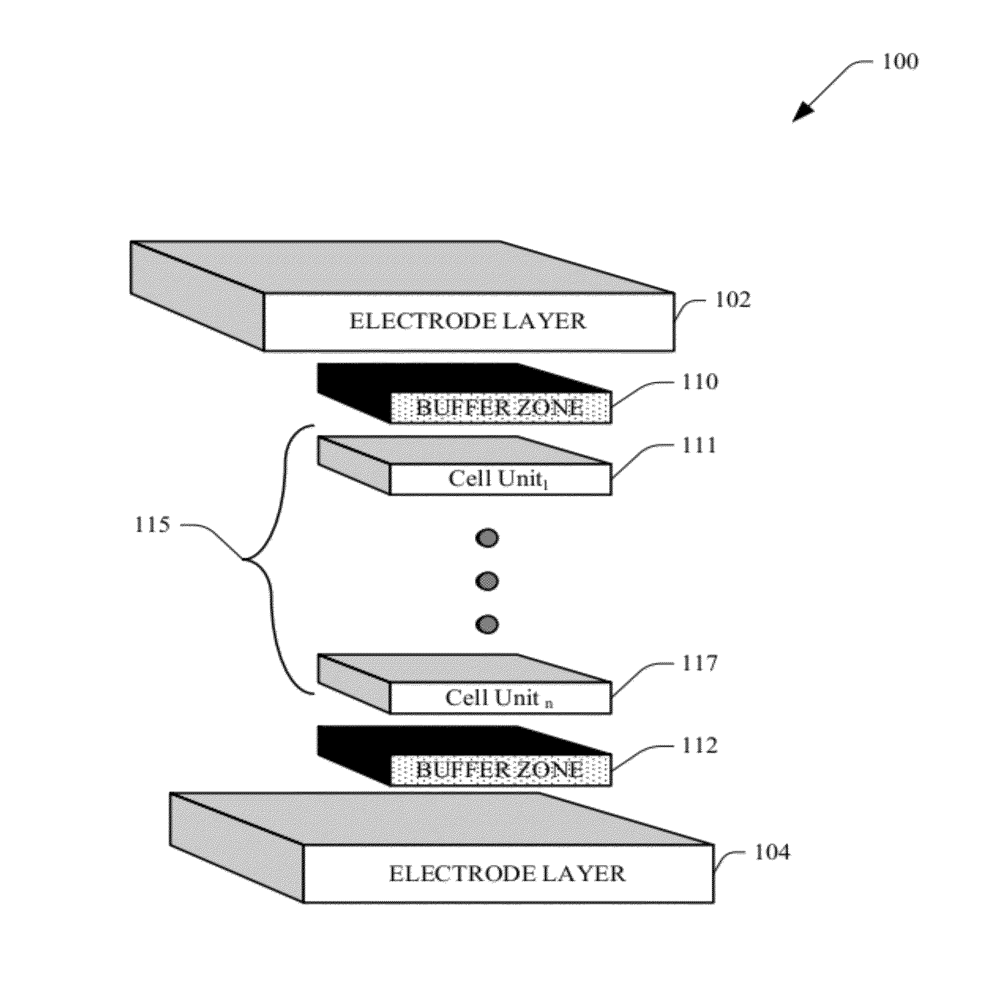
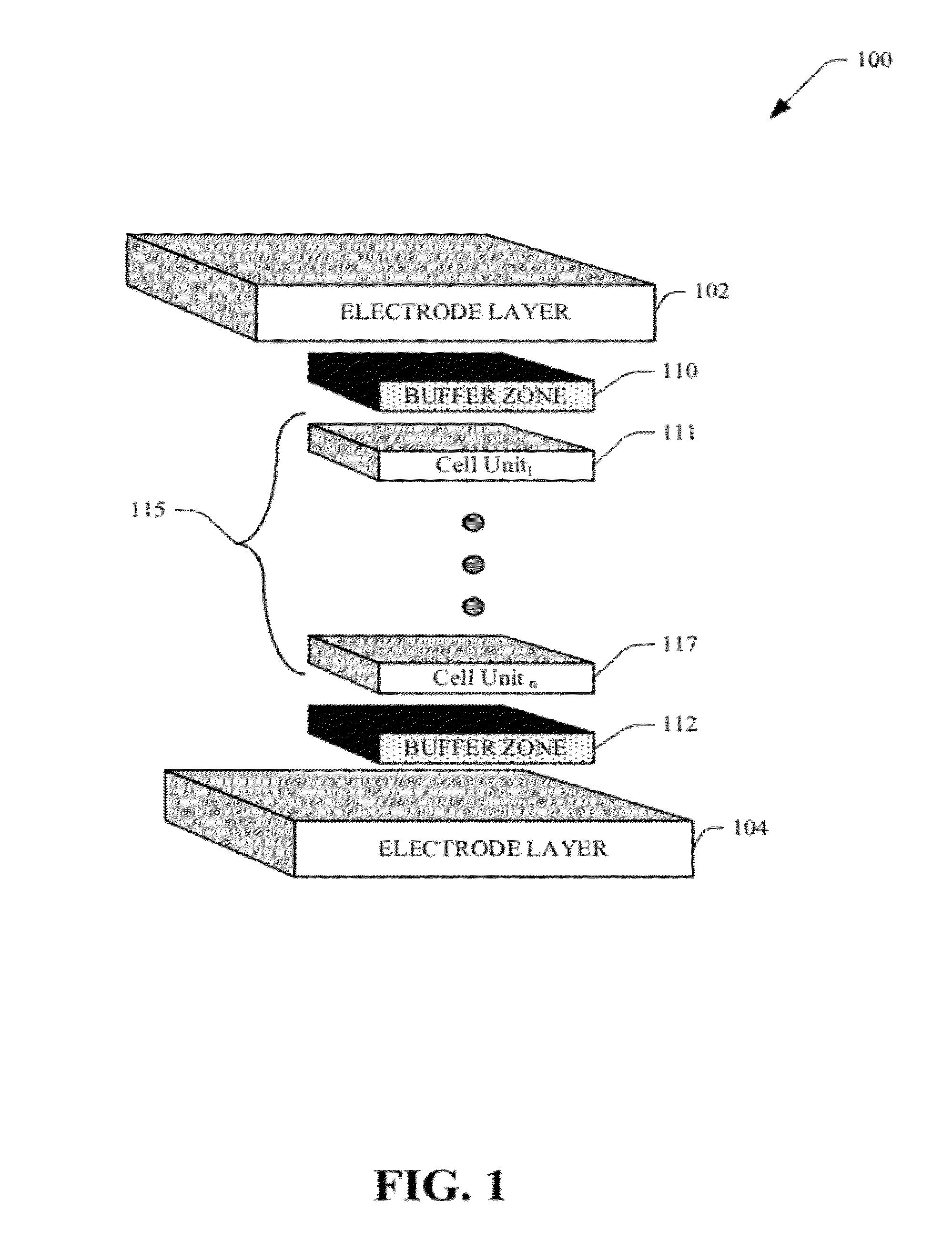
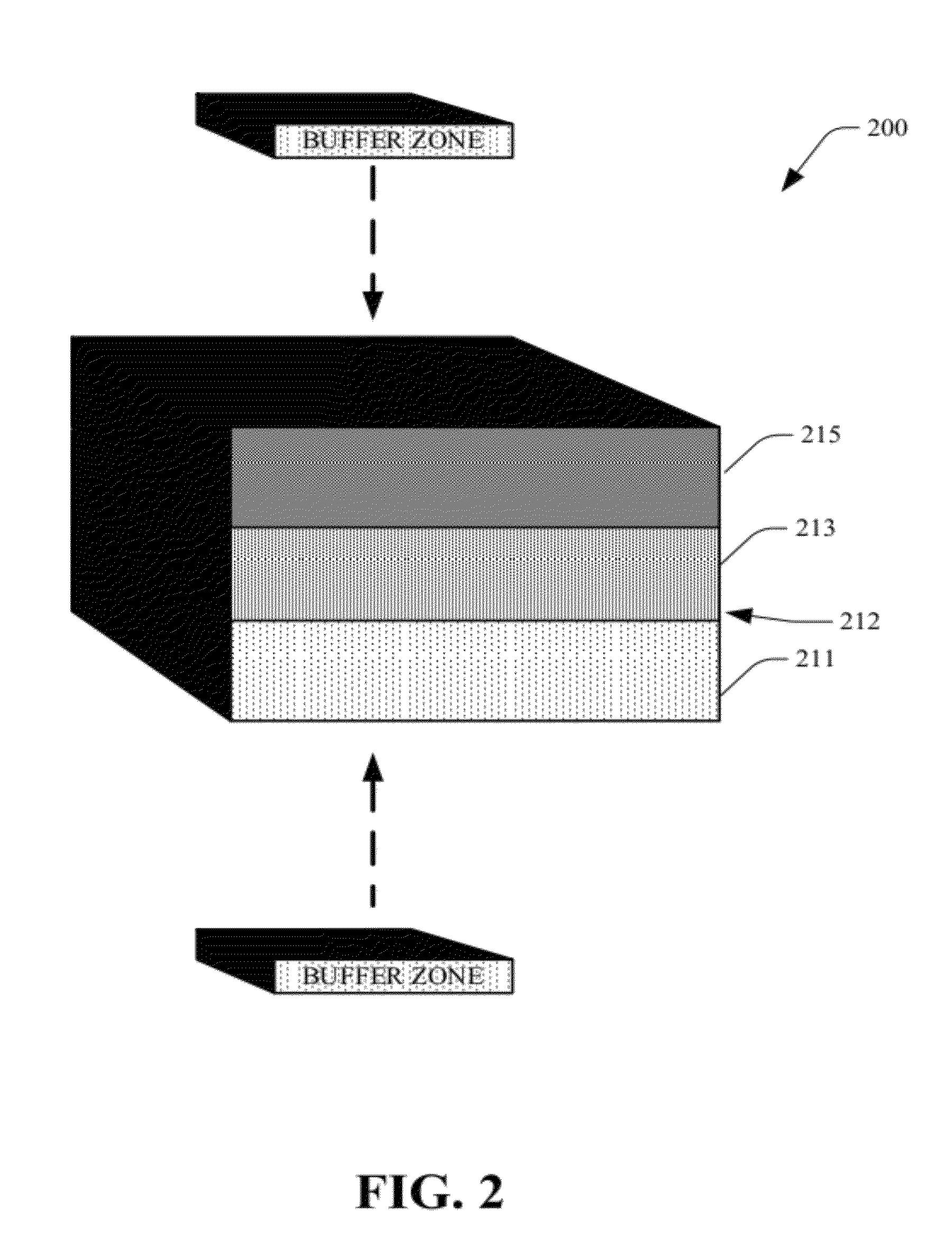
[0020]FIG. 1 illustrates a schematic block diagram of an arrangement for buffer zones as part of vertical multi junction (VMJ) cell in accordance with an aspect of the subject innovation. The VMJ 115 itself is formed from a plurality of integrally bonded cell units 111, 117 (1 to n, n being an integer), wherein each cell unit itself is formed from stacked substrates or layers (not shown). For example, each cell unit 111, 117 can include a plurality of parallel semiconductor subs...
PUM
 Abstract
Description
Claims
Application Information
 - R&D
- Intellectual Property
- Life Sciences
- Materials
- Tech Scout
- Unparalleled Data Quality
- Higher Quality Content
- 60% Fewer Hallucinations
Browse by: Latest US Patents, China's latest patents, Technical Efficacy Thesaurus, Application Domain, Technology Topic, Popular Technical Reports.
© 2025 PatSnap. All rights reserved.Legal|Privacy policy|Modern Slavery Act Transparency Statement|Sitemap|About US| Contact US: help@patsnap.com