Charge-coupled photovoltaic devices

Inactive Publication Date: 2012-03-01
MANCHANDA LALITA
View PDF9 Cites 10 Cited by
  • Summary
  • Abstract
  • Description
  • Claims
  • Application Information

AI Technical Summary

Benefits of technology

[0013]In an aspect of the invention, a photovoltaic solar cell (also “photovoltaic” herein) device invokes a device structure with charge coupling by quantum tunneling through an insulator to reduce losses, such as thermalisation, recombination and reflection losses.
[0019]EI may be greater than or equal to EI-II. In some situations, EI-I may be greater than EI-II. Light incident on the photovoltaic device may pass through the transport semiconductor layer to layer I-II, which may absorb photons with energy greater than or equal to EI-II. The remainder of the energy is transferred through this layer and the quantum coupling layer to device II, where further carriers are generated. The coupling layer couples electrons from device II to device I and quenches the positive charges generated in the absorbing layer I-II. The device I absorbs high energy photons and transports high energy carriers and reduces the generation of high carriers in device II and thus reduces the thermalisation loss in device II and increases the net efficiency. Also, by reducing the generation of high energy electrons in device II, the net heat generation in device II may be reduced and the operating efficiency of device II may be improved, providing for further reduction of the thermalisation loss. The layers I-I and I-II may be two separate layers and / or intermixed with band gaps EI-I and EI-II, wherein EI-I may be greater than or equal to EI-II. In some situations, EI-I may be greater than EI-II.
[0024]A photovoltaic device may have a three dimensional topography to increase the absorption coefficient in the device I and device II and to decrease the electron transfer loss in the transport layer. Such topography may include a corrugated surface having variously oriented crystallographic facets. The three dimensional structure may be a V-Groove or Via or Cylinder shape or random rough surface with aspect ratio optimized for maximum photon absorption and to keep the electric field on the coupling layer less than the breakdown strength of the coupling insulator. The three dimensional structure reduces reflection (improves the photon absorption), increases quantum charge coupling and reduces the effective amount of silicon / semiconductor used to make the device II.
[0026]Device I may be formed of one or more charge coupling layers. In some cases, Device I and Device II may be formed in a 3D configuration, which may increase photon absorption.

Problems solved by technology

While, emerging nanowire silicon is also a bulk silicon technology, the η×R / C trend of this technology has yet to be established.
These are expensive technologies with market limited to space applications and the emerging CPV systems.
However, scarcity of the available raw materials and the toxicity of Cd may make it difficult to capture large scale markets.
One drawback of amorphous silicon is that it does not have a very high efficiency and light induced degradation reduces the figure of merit for amorphous and micromorph technologies.
However, chemical instability is a bottleneck to put it in the market place.
However, the fundamental and technology related losses have limited the maximum achieved cell efficiency to about 25% at the lab level and about 18% at the industry (or module) level.
Current solar cells suffer from other limitations, such as energy losses (or losses).
Loss by reflection is a technology or design related loss where part of the incident photon flux is reflected by the device surface.
Loss due to incomplete absorption is also a technology or design related loss due to the limited thickness and large wavelength photons not being completely absorbed.
Loss due to metal coverage is a design-related loss and depends on the cell front and back metal coverage.
Other losses that may limit solar cell efficiency include transmission losses, thermalisation loss and recombination losses.
Thermalisation loss includes loss due to excess energy of photons.
While very high lifetime substrates are available, high lifetime silicon substrates are very expensive.
Interface and bulk recombination loss therefore remains to be a major technology challenge for silicon and other solar cell technologies.

Method used


Image

  • Charge-coupled photovoltaic devices
  • Charge-coupled photovoltaic devices
  • Charge-coupled photovoltaic devices

Examples


Embodiment Construction

[0049]While preferable embodiments of the present invention have been shown and described herein, it will be obvious to those skilled in the art that such embodiments are provided by way of example only. Numerous variations, changes, and substitutions will now occur to those skilled in the art without departing from the invention. It should be understood that various alternatives to the embodiments of the invention described herein may be employed in practicing the invention. It is intended that the following claims define the scope of the invention and that methods and structures within the scope of these claims and their equivalents be covered thereby.

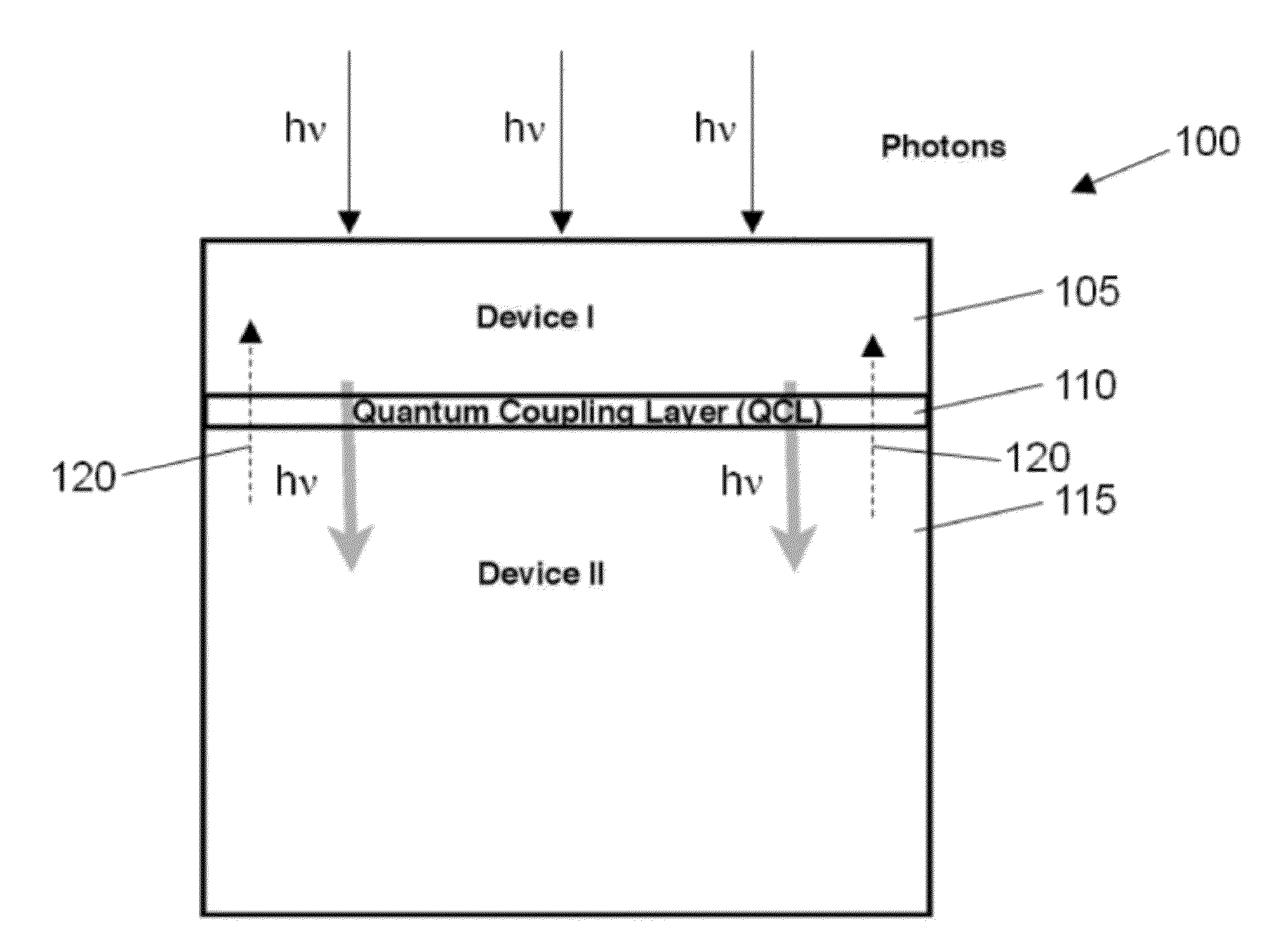
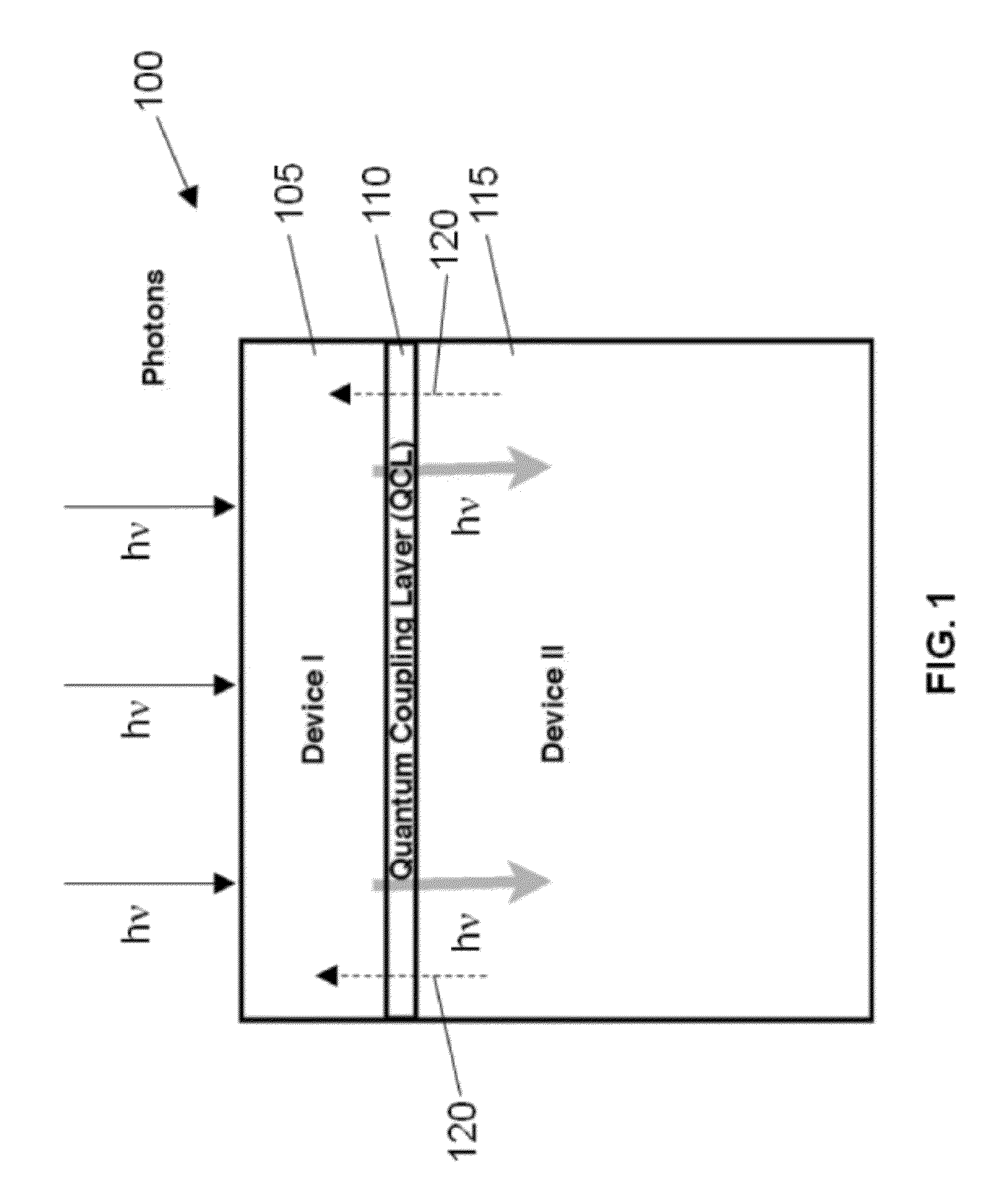
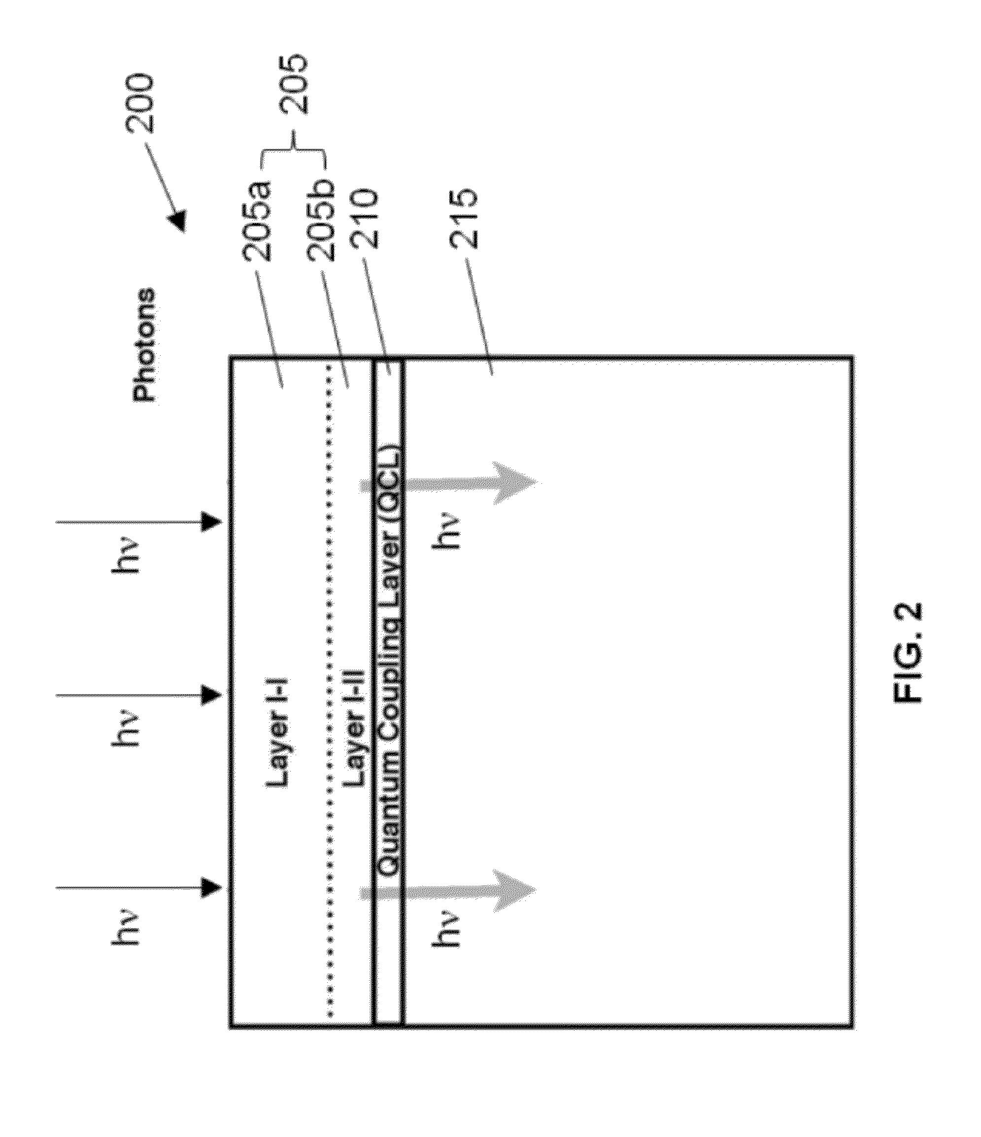
[0050]Photovoltaic devices and cells described various embodiments of the invention may improve charge generation and retention over current devices and cells. Photovoltaic cells described in various embodiments may advantageously increase the amount of charge generated per given quantity of light incident on a photovoltaic device. P...


PUM


Abstract

A photovoltaic (solar) cell comprises two photovoltaic devices that are quantum mechanically coupled via a charge-coupling layer. One of the PV devices may have an energy band gap that is larger than or equal to an energy band gap of the other of the PV devices. The effective electron barrier heights or electron affinity on side portions of the quantum coupling layer are higher than the maximum energy of photo-generated electrons in the photovoltaic devices. The photovoltaic device with larger band gap may include an electron and / or hole transport layer and photon absorbing layer. Photons are transmitted through the transport layer to the absorbing layer. Some high energy photons are absorbed by the absorbing layer. The absorbing layer may function as an absorber of high energy photons and generator of electrons / holes (or excitons). Holes generated in the absorbing layer may be quenched by electrons from the second photovoltaic device.

Description

BACKGROUND OF THE INVENTION[0001]The photovoltaic effect may be used to convert sunlight (photons) to electricity. When photons strike a photovoltaic, solar device, or cell (e.g., a or series of semiconductor p-n junctions), photons may be partially absorbed and partially reflected. Absorption of photons by a solar cell may result in generation of electron-hole pairs (EHP). EHPs, once separated across a p-n junction or band-offsets, result in the generation of voltage which may generate current in an external load. Therefore, power may be extracted from the photovoltaic device.[0002]Solar or photovoltaic cells (also “cells” herein) may be configured in arrays to make solar cell systems (also “modules” herein). The net power generation from a module is directly proportional to the efficiency (η) of the solar cell. This efficiency may depend on the fundamental properties of the photon absorbing and electron transporting layers, cell design configured for electrons paths, and the techn...

Claims


Application Information

Patent Timeline
IPC IPC(8): H01L31/042H01L31/06
CPCB82Y20/00Y02E10/547H01L31/035245H01L31/035281H01L31/03685H01L31/03762H01L31/068H01L31/0687H01L31/072H01L31/0725H01L31/075H01L31/076H01L31/1804H01L31/202Y02E10/544Y02E10/545Y02E10/548H01L31/035236Y02P70/50
Inventor MANCHANDA, LALITA
Owner MANCHANDA LALITA
Why Eureka
Try Eureka