Mos device for eliminating floating body effects and self-heating effects

Inactive Publication Date: 2012-02-02
SHANGHAI INST OF MICROSYSTEM & INFORMATION TECH CHINESE ACAD OF SCI
View PDF50 Cites 7 Cited by
  • Summary
  • Abstract
  • Description
  • Claims
  • Application Information

AI Technical Summary

Benefits of technology

[0010]A method of manufacturing a MOS device for eliminating floating body effects and self-heating effects, the method comprises: (a) according to priority epitaxial growing a SiGe layer and a Si layer on a Si substrate; (b) forming a first conduction type SiGe layer and a first conduction type Si layer on the Si substrate by etching and doping the SiGe layer and the Si layer, wherein the first conduction type Si layer is used for forming an active region; (c) coating photo resist layer on the first conduction type Si layer to cover the surface of a first region used for forming a gate channel, which spreads outwards from both sides to cover partial sidewalls of the first conductive SiGe layer under this region, then removing a part of the first conduction type SiGe layer under the first conduction type Si layer by selective etching, thus forming a SiGe isolation layer, so that the areas for forming source region and drain region are suspended; (d) removing the photo resist layer, and filling insulating medium around the SiGe isolation layer above the Si substrate and the first conduction type Si layer; (e) forming a gate region above the first conduction type Si layer, and forming a source region and a drain region with a second conduction type in the first conduction type Si layer by doping process to finish fabrication of the MOS device.

Problems solved by technology

However, the buried oxide layer (BOX) in a SOI structure presents two major challenges to a SOI device's performance and reliability.
The first issue is the floating body charge effect and self-heating effects in SOI devices, which can lead to the devices performance degeneration and serious influences on the device reliability.
With the size of the device continuing to shrink, the negative influence will be more prominent, thus greatly limiting the promotion of SOI technique.
In this case, the buried oxide layer in a SOI device isolates the body region from the device, and charges generated from impact ionization cannot be quickly released.
As a result, SOI devices have a tendency to accumulate charges and float electrically.
In addition, the buried oxide layer in a SOI device has relatively low thermal conductivity which results in device self-heating.
When the SOI device works, the buried oxide layer has high thermal resistance, and the device temperature is too high, thus affecting the device performance.
However, the device's manufacture process is very complicated.
The level of complexity in this process hinders continued device shrinking in the future.

Method used


Image

  • Mos device for eliminating floating body effects and self-heating effects
  • Mos device for eliminating floating body effects and self-heating effects
  • Mos device for eliminating floating body effects and self-heating effects

Examples


Embodiment Construction

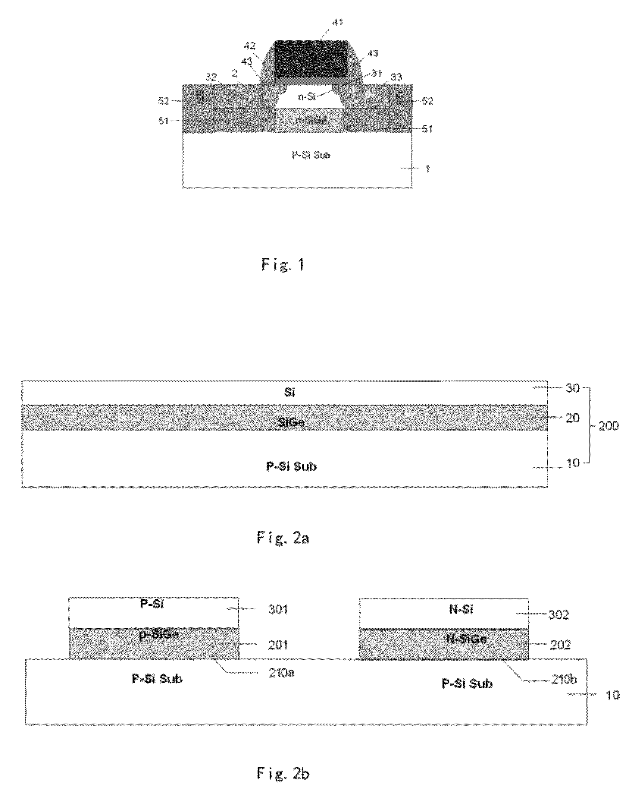
[0013]The present disclosure is further explained in detail according to the accompanying drawings.

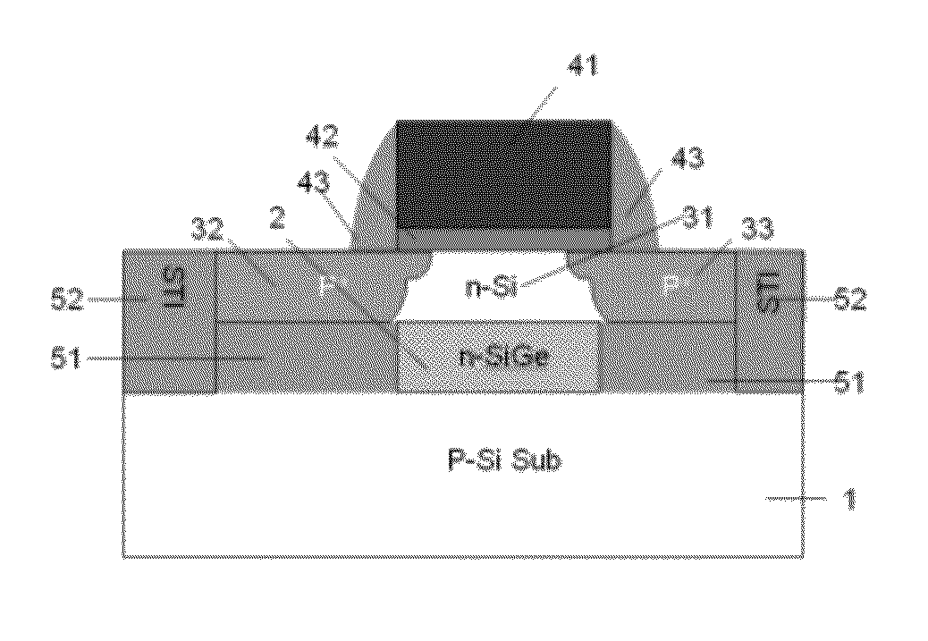
[0014]FIG. 1 provides a cross sectional view of a MOS device for eliminating floating body effects and self-heating effects. The MOS device includes a Si substrate 1; an active region located on the Si substrate 1, the active region includes a gate channel 31, a source region 32 and a drain region 33, and the source region 32 and the drain region 33 are located at the two opposite ends of the gate channel 31; a gate region located over the gate channel 31, including a gate dielectric layer 42 and a gate electrode 41 provided on the gate dielectric layer 42, wherein a pair of insulation spacers 43 is provided around the gate region; a shallow trench isolation (STI) region 52 is located surrounding the active region.

[0015]A buried insulation layer 51 is formed in the second space between the source region 32 and the Si substrate 1 to electrically isolate them, and in the third space betw...


PUM


Abstract

A SOI MOS device for eliminating floating body effects and self-heating effects are disclosed. The device includes a connective layer coupling the active gate channel to the Si substrate. The connective layer provides electrical and thermal passages during device operation, which could eliminate floating body effects and self-heating effects. An example of a MOS device having a SiGe connector between a Si active channel and a Si substrate is disclosed in detail and a manufacturing process is provided.

Description

FIELD OF THE INVENTION[0001]The present invention relates to semiconductor MOS device, and particularly, to a MOS device for eliminating floating body effects and self-heating effects, and a manufacturing method thereof.BACKGROUND OF THE INVENTION[0002]SOI means silicon on insulator. In SOI technique, the speed of silicon on insulator (SOI) devices is significantly improved compared to traditional bulk silicon devices, owing to reduced source and drain parasitic capacitance. Other advantages of SOI devices include improved shot-channel effect, latch-up prevention, and simpler device manufacturing. SOI devices also demonstrate high speed, low power consumption, high integration density, and high reliability. As a result, SOI has become one of the mainstream IC technologies.[0003]However, the buried oxide layer (BOX) in a SOI structure presents two major challenges to a SOI device's performance and reliability. The first issue is the floating body charge effect and self-heating effect...

Claims


Application Information

Patent Timeline
IPC IPC(8): H01L29/80H01L21/337
CPCH01L21/823807H01L21/823878H01L21/84H01L29/78612H01L29/0653H01L29/1054H01L27/1207
Inventor HUANG, XIAOLUCHEN, JINGWANG, XIXIAO, DEYUAN
Owner SHANGHAI INST OF MICROSYSTEM & INFORMATION TECH CHINESE ACAD OF SCI
Why Eureka
Try Eureka