
Method of Manufacturing and Operating an Antenna Arrangement for a Communication Device

a technology for communication devices and antennas, applied in the field of electronic communication devices, can solve the problems of inability to reuse or recover excess waste of adhesive-coated metal foil, inability to recover substantial waste of expensive raw materials, and inability to manufacture and operate antennas. to achieve the effect of simple or complex antenna design

Inactive Publication Date: 2011-12-15
ILLINOIS TOOL WORKS INC
View PDF0 Cites 33 Cited by
  • Summary
  • Abstract
  • Description
  • Claims
  • Application Information

AI Technical Summary

Benefits of technology

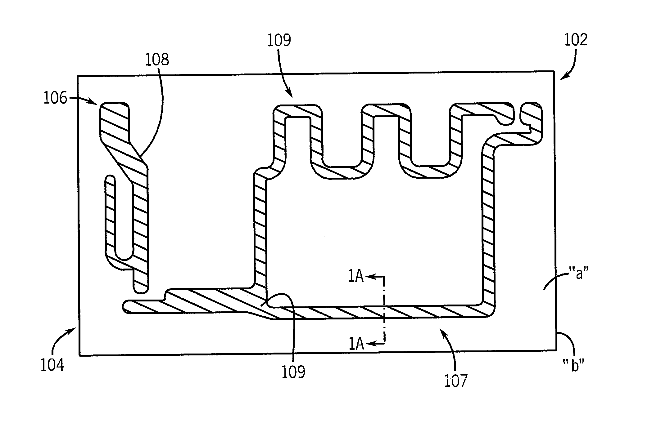
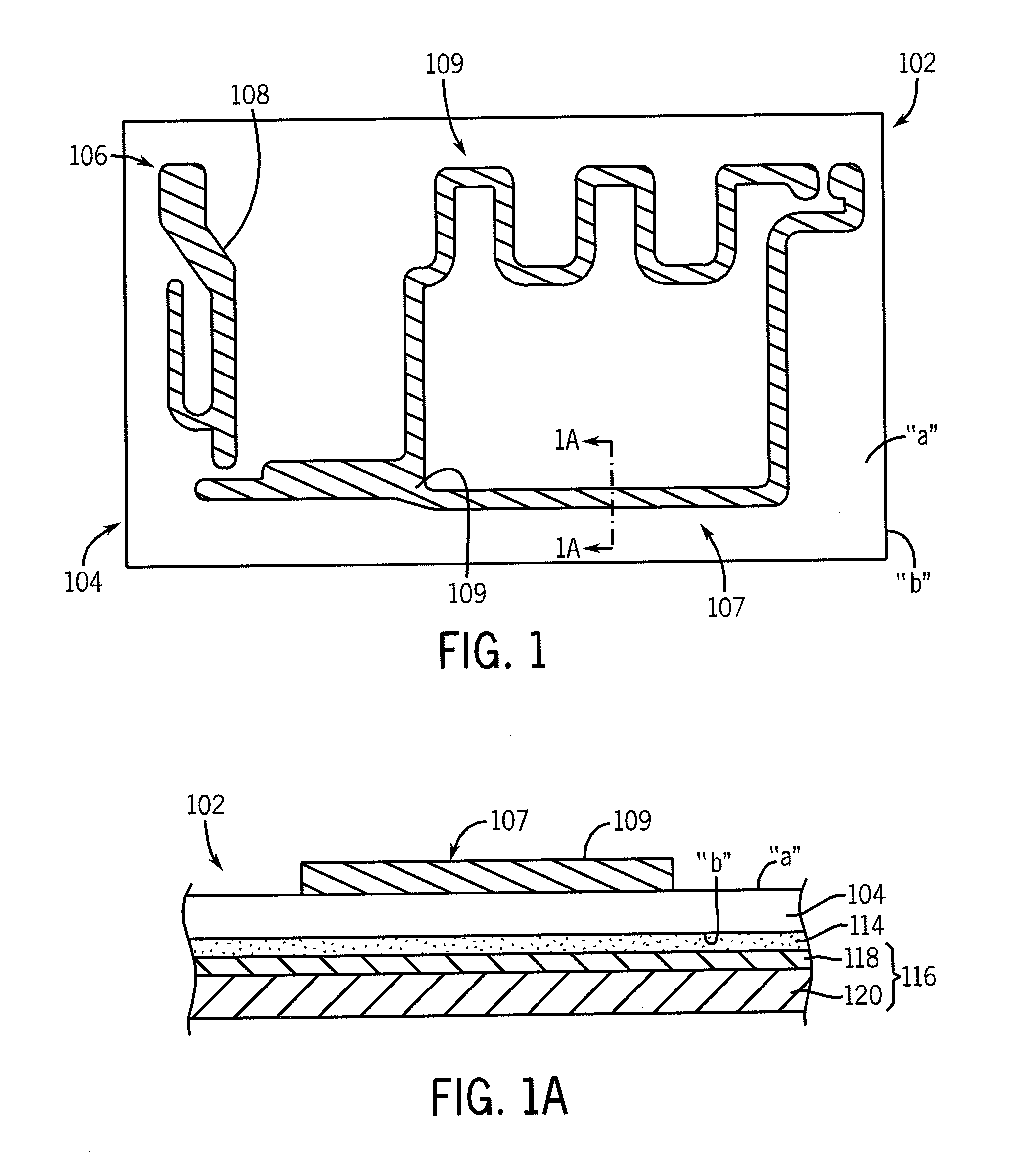
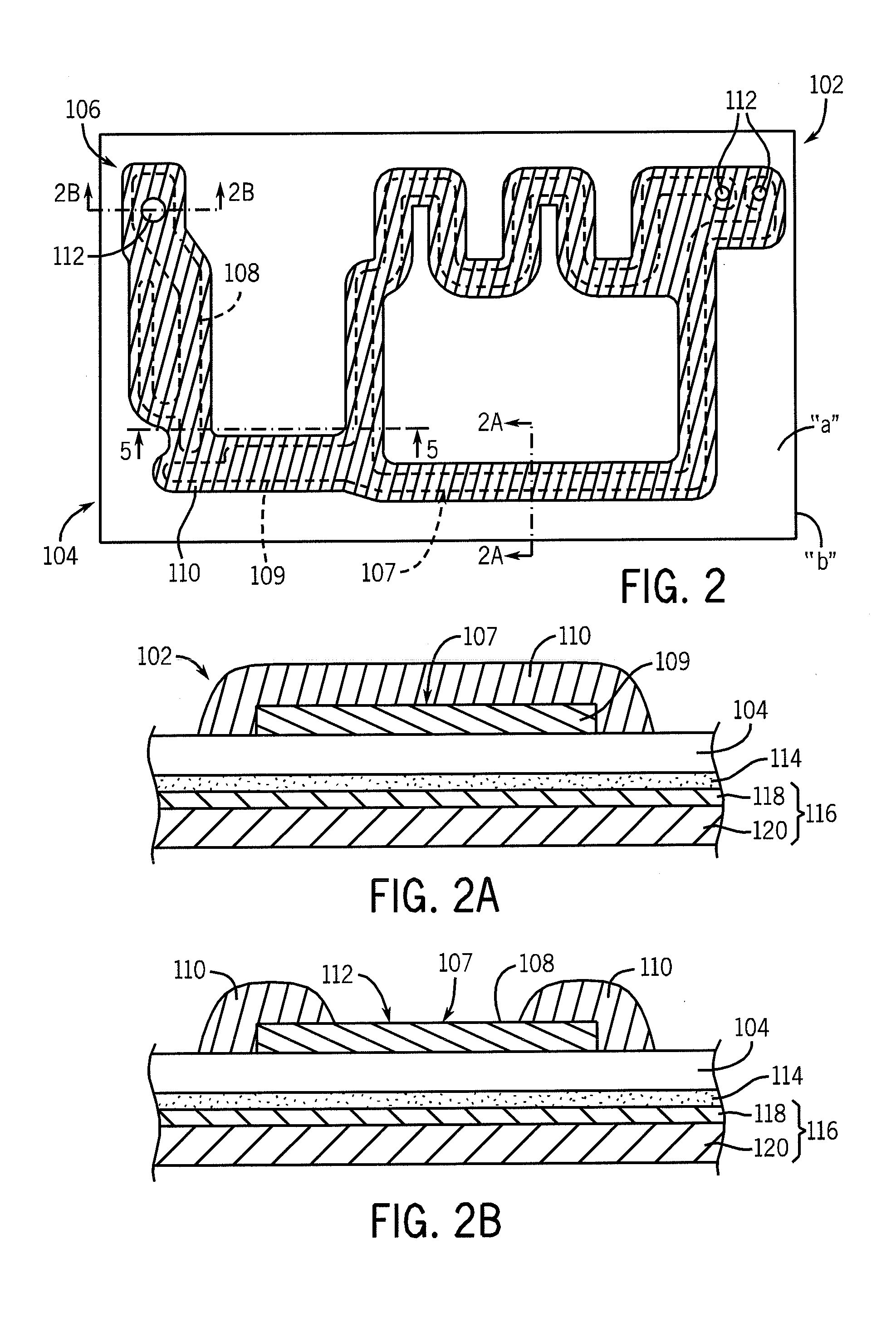
[0017]The invention also relates to a method of fabricating an arrangement or designs of antennas. In an embodiment of the method, an antenna design is prepared by forming an electrically conductive material on the surface of a flexible dielectric substrate to form a simple or complex antenna design. The method further includes applying a compatible dielectric material, which preferably functions as a moisture barrier, over the simple or complex antenna design to conform to and substantially match and encapsulate the antenna design on the substrate, wherein the antennas are functional to transmit and / or receive communication signals within multiple frequency bands, which are preferably non-contiguous bands.
[0018]An antenna formed according to the invention is initially formed as encapsulated conductive traces laid on a dielectric substrate (usually polymer film). As the integral part of an electronic device, this antenna can be attached to the mechanical carrier within the device so that its conductive traces remain all in one plane, or it can be attached so that its conductive traces form a simple or complex 3-dimensional shape.
[0021]In an embodiment of a method according to the invention, an antenna arrangement is prepared by (a) applying (e.g., printing) a liquid formulation (e.g., “conductive ink”) that is a precursor to a solid conductive material on the surface of a flexible dielectric substrate to form a simple or complex antenna design which, in some embodiments, can include a first subset antenna design, a second subset antenna design, etc.; (b) curing the liquid formulation to convert the liquid into an electrically conductive solid material to form a solid antenna design, for example, by infrared (IR) heating, inductive heating or other suitable heating process, or by ultraviolet (UV), visible or other high energy radiation, etc.; (c) applying (e.g., printing) a compatible fluid (e.g., “dielectric ink”) that is a precursor to a solid dielectric material, which is (when cured) preferably moisture impenetrable, over the solidified antenna design to conform to and substantially match the subset antenna designs; and (d) curing the precursor dielectric material such that the subset antenna designs are encapsulated between the dielectric substrate and a solid, preferably moisture impenetrable, dielectric material.

Problems solved by technology

In the case of FPCBs, the metal foil is typically subjected to etching and plating baths that generate substantial chemical waste.
The metal foil that is chemically etched away cannot be recovered and therefore generates a substantial waste of expensive raw materials.
However, with this technology, substantial portions of the expensive adhesive pre-coated metal foil are cut away to form the conductors for the antenna, resulting in excess waste of adhesive-coated metal foil that cannot be re-used or recovered.
Such methods require very tight antenna cutting and bending tolerances, and very tight phone case tolerances.
In addition, manufacturing antennas by die-cutting metal foil has reached limitations in cutting intricate small dimensions and sharp angle patterns, such that with the new technological advancements, the effort expended on the quality control and amount of defective products have shown an upward trend.

Method used


Image

  • Method of Manufacturing and Operating an Antenna Arrangement for a Communication Device
  • Method of Manufacturing and Operating an Antenna Arrangement for a Communication Device
  • Method of Manufacturing and Operating an Antenna Arrangement for a Communication Device

Examples


example

[0086]Present metal foil antennas, both etched in a flexible PCB or die-cut, are often covered with an insulative film or coating to prevent scratching and tearing of the metal foil. The thin insulative film is glued onto the metal foil and is chosen to meet mechanical requirements, not electrical requirements. The insulative film covers the entire antenna, often resulting in a high loss tangent.

[0087]In the present example, two commercially available cellular telephones were tested for the radiation efficiency of their secondary antennas. One telephone was tested only at FM (88-103 MHz) frequencies and the other telephone was tested at FM, Global Positioning Satellite (1.575 GHz) and Bluetooth (2.4 GHz) frequencies. In both cases, tests were made with antennas manufactured by screen printing conductive ink consisting of dispersed silver particles in a polymeric binder on dielectric film substrate. In one case, the printed antennas were left uncovered and in the other case, the prin...


PUM

PropertyMeasurementUnit
Frequencyaaaaaaaaaa
Dielectric polarization enthalpyaaaaaaaaaa
Lengthaaaaaaaaaa

Abstract

Thin, flexible antenna arrangements for use in communication devices, such as mobile communications devices, and methods of making and using the antenna arrangements are provided. The methods used to make the antenna arrangements are print-based and provide a simplified procedure, with a reduced number of process steps, the use of fewer materials and the production of less material waste than conventional methods based on etching and die cutting.

Description

FIELD OF THE INVENTION[0001]The present invention relates to the field of electronic communication devices, and more particularly, to antennas for mobile communication devices and antennas for WLAN, FM, AWS, WiMax, LTE, Bluetooth, UHF, VHF, Media FLO, Land Mobile, Cognitive Radio, Wireless Microphone, PCS, GSM, ZigBee, CDMA, iDEN, UWB, Amateur Radio, Point-to-Point, Television, radar, satellite, and radio frequency communication between different pieces of equipment, including, but not limited to, medical equipment and patient monitoring devices, office equipment, electronic meeting communication devices, entertainment devices, manufacturing machinery, automobile functions, monitoring devices, home and restaurant appliances, electric and gas distribution and metering devices, gambling machinery and equipment, and livestock monitoring devices.BACKGROUND OF THE INVENTION[0002]The use of mobile electronic communication devices has increased dramatically. As a result, mobile devices suc...

Claims


Application Information

Patent Timeline
IPC IPC(8): H01Q1/38H01P11/00H01Q21/28
CPCY10T29/49016H01Q21/0087H01Q1/24H01Q1/38
Inventor DJORDJEVIC, MIOMIR B.MEITZLER, WILLIAM H.DE WILDE, IGNATIUS GERARDUS T.JELONEK, PAUL R.CHU, TUN-JEN
Owner ILLINOIS TOOL WORKS INC
Learn More