
Mixed alloy solder paste

Active Publication Date: 2011-11-03
INDIUM CORPORATION
View PDF2 Cites 17 Cited by
  • Summary
  • Abstract
  • Description
  • Claims
  • Application Information

AI Technical Summary

Benefits of technology

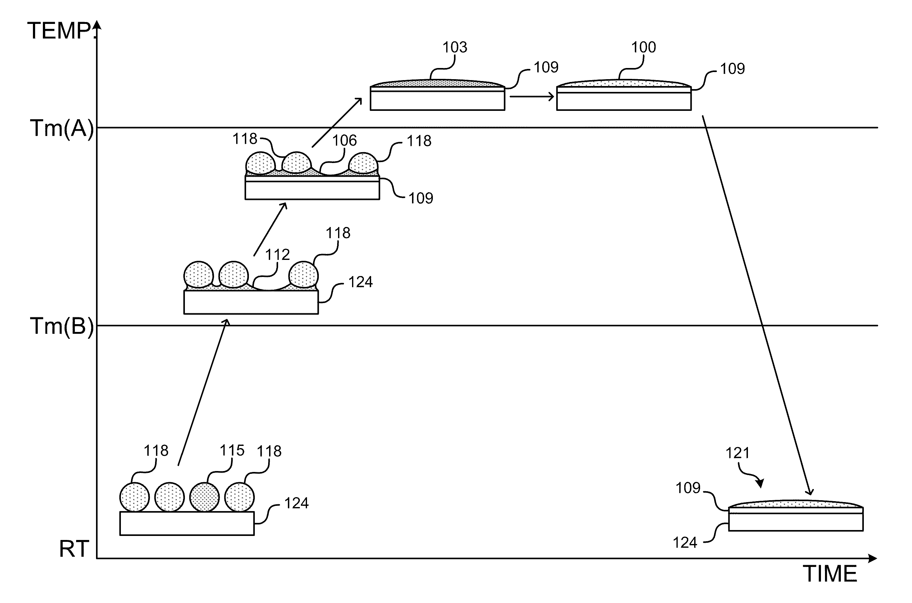
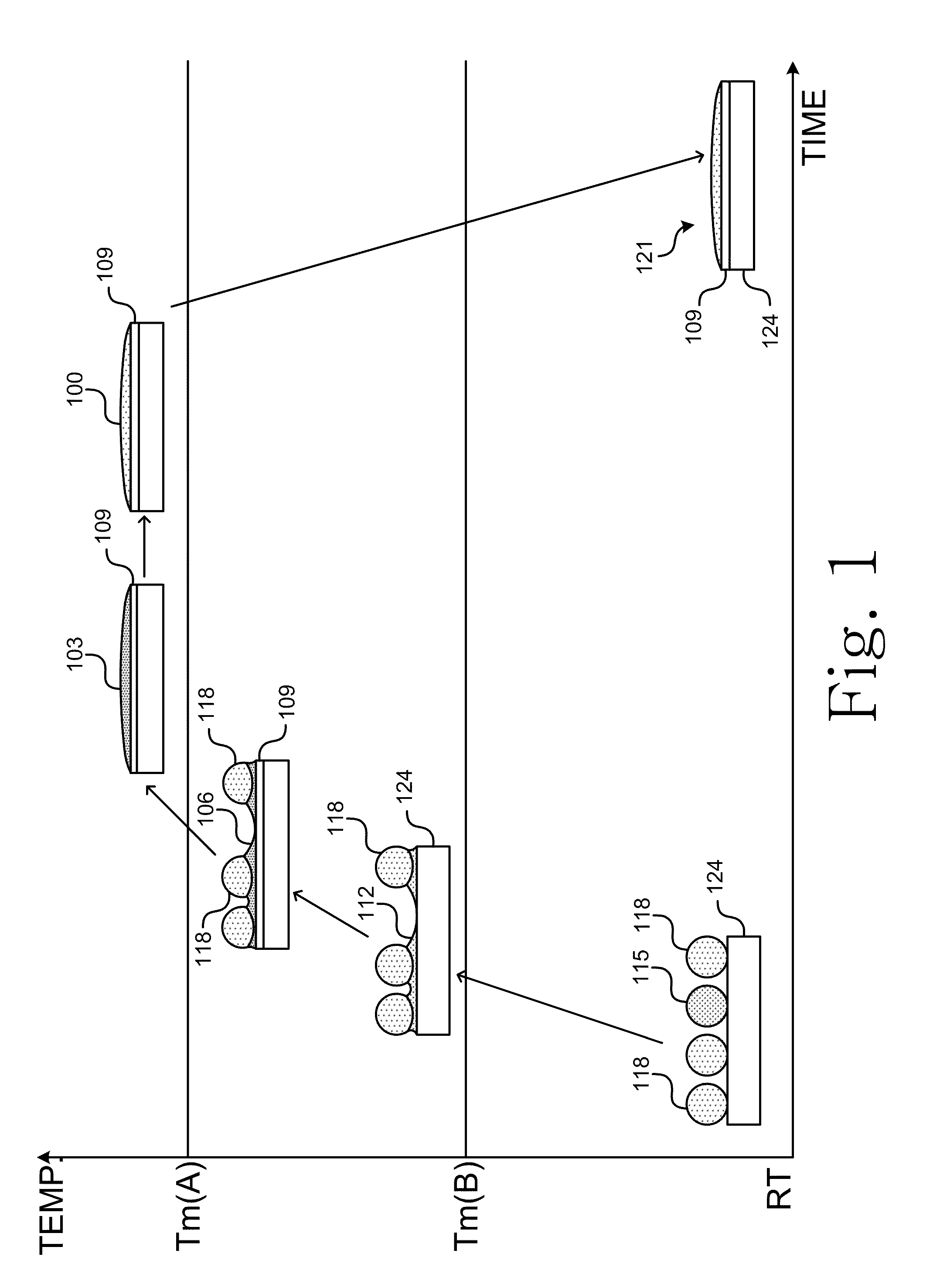
[0012]The present invention claims a new technology for designing and preparing mixed alloy solder pastes, which deliver the combined merits from the constituent alloy powders. In some embodiments, the mixed alloy solder pastes are suitable for high-temperature solder applications such as die attach because the constituents provide the desired merits including improved reaction chemistry, well-controlled IMC layer thickness, and the enhanced reliability accordingly from the second alloy and the high melting temperature and good thermal / electrical conductivity from the first alloy. The invention also presents the method of preparing the mixed alloy solder pastes and the methodology of joining the electronic components or mechanical parts with the mixed alloy solder pastes.
[0013]The invented technology provides a method of designing mixed alloy powder pastes, in which the additive powders are present in the paste to improve the reaction chemistry at a relatively lower temperature or together with the melting of the first alloy solder powders. In some embodiments, the mixed alloy powder pastes include two or more alloy powders and a flux. The alloy powders in the paste are composed of one solder alloy powder as a majority and an additive alloy powder as a minority. The additives provide the superior chemistry to wet on various metallization surface finishes of the substrates, namely the commonly used Cu and Ni surface finishes, etc.
[0014]In some embodiments, the additives will melt before or together with the melting of the majority solder. The molten additives will wet on and adhere to the substrate before or together with the partially or completely molten first alloy. The additives are designed to dominate the formation of IMCs along the substrate metallization surface finish and be completely converted into IMCs during the reflow process. The thickness of the IMC layer will thus be well controlled by the quantity of the additives in the paste because of the dominant roles the additives play in the IMC formation. In some embodiments, the first alloy solder will have a strong affinity to the IMC layer formed between the additives and the substrate. This strong affinity will enhance the bonding strength between the solder body and the IMCs. Thus, the desired reaction chemistry and the well controlled thickness of the IMC layer not only improves the wetting performance but also enhances the bonding strength associated with the wetting performance.

Problems solved by technology

Lead generated by disposal of electronic assemblies is considered hazardous to the environment and human health.
Currently, there are no drop-in lead-free alternatives available in the industries.
But their solidus temperature is no higher than 250° C., which can not satisfy the 260° C. requirement for reflow resistance.
Zn-based alloys, including eutectic Zn—Al, Zn—Al—Mg, and Zn—Al—Cu, have melting temperature above 330° C. However, the high affinity of Zn, Al, and Mg to oxygen causes extremely poor wetting on various metallization surface finishes.
However, problems arise when the semi-solid solder is compressed inside an encapsulated package and forces the semi-solid solder to flow out.
This creates a risk of unexpected functional failure.
The existence of the IMC layer and its intensive growth during the subsequent reflow and operation also causes reliability concerns.
However, extremely high cost restricts its application within the fields where cost overcomes reliability considerations.
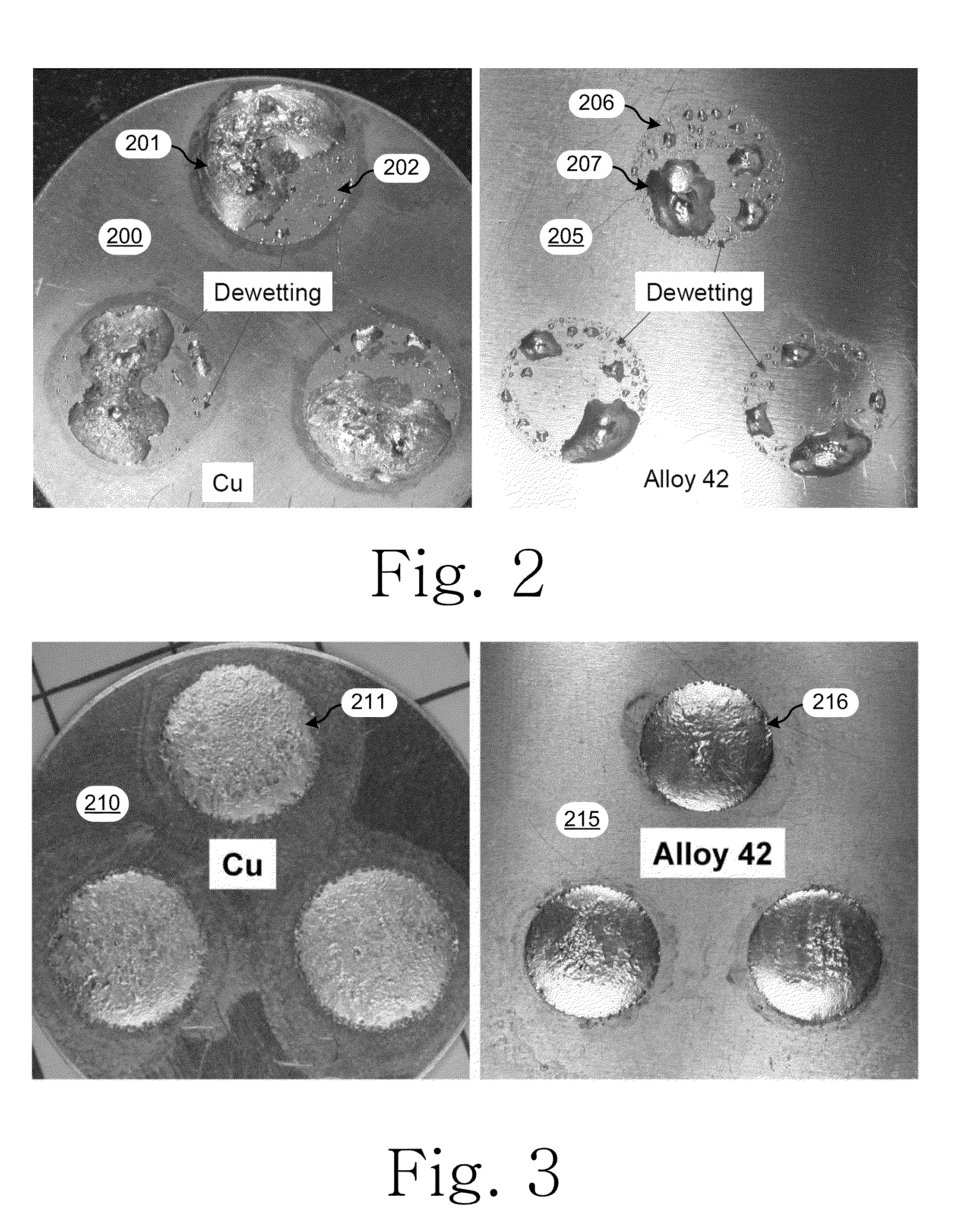
However, there are a few major concerns: (1) poor wetting on various surface finishes and (2) the associated weak bonding interface originating from the poor wetting.
The melting temperature requirement for high melting lead-free solders makes Sn—Sb and Zn—Sn solders unsuitable.
The extremely high cost of Au rich solders limits their acceptance by the industry.
However, their poor wetting, due to high affinity to oxygen (in the Zn—Al solder system) or due to poor reaction chemistry between the solder and the substrate metallization (in the Bi—Ag solder system or even some lead-containing solders such as the Pb—Cu and Pb—Ag systems), makes these high melting solders hard to use in the industry because of the weak bonding strength resulting from the poor wetting.
As described above, the poor wetting of a solder originates from (1) poor reaction chemistry or (2) the oxidation of the solder.
For example, the poor wetting of Bi-based solder on different metallization surfaces results mainly from the poor reaction chemistry between Bi and the substrate materials (i.e. Cu) or the oxidation of Bi during reflow.
However, this doping will not change the reaction chemistry between Bi and the metallization surface finish of the substrate.
Bi and Ni will form IMC layer between a Bi / Ni interface, but the brittle IMCs (Bi3Ni or BiNi) weaken the joint strength because cracks always grow along either the interface between Bi3Ni and the solder matrix or the interface between BiNi and the Ni substrate.
Accordingly, the reaction chemistry between Bi and substrate materials result in the poor wetting and the weak bonding strength.
However, alloying is normally associated with some unexpected property loss.
However, directly alloying Sn into BiAg (where the Ag is aimed at increasing the thermal / electrical conductivity) could cause (1) significant decrease in the melting temperature or (2) the formation of Ag3Sn IMC in the alloy.
This will not improve the reaction chemistry between Sn with substrate metals if there is no enough time for them to be dissolved in the molten solder during reflow.
Thus, alloying elements directly into solder, such as Sn directly into Bi—Ag alloys, reveal minimal improvements.

Method used


Image

  • Mixed alloy solder paste
  • Mixed alloy solder paste
  • Mixed alloy solder paste

Examples


example

[0063]Various mixed alloy powder solder pastes that span the ranges described herein, were tested for solder performance.

[0064]Table 1 describes formulations of example mixed solder pastes made using a first alloy comprising Bi11Ag or Bi2.6Ag, a second alloy comprising Sn10Ag25Sb or Sn10Ag10Sb, and flux.

TABLE 1Weight percentages of mixed solderalloys using Group A second alloysBi11AgBi2.6AgSn10Ag25SbSn10Ag10SbSn15SbFlux80 wt %10 wt % 10 wt %82 wt %8 wt %10 wt %84 wt %6 wt %10 wt %86 wt %4 wt %10 wt %42 wt %42 wt %6 wt %10 wt %86 wt %4 wt %10 wt %84 wt %6 wt %10 wt %86 wt %4 wt %10 wt %

[0065]Table 2 describes formulations of example mixed solder pastes made using a first alloy comprising Bi11Ag, a second alloy comprising Sn3.8Ag0.7Cu, Sn3.5Ag, Sn0.7Cu, or Sn9Zn, and flux.

TABLE 2Weight percentages of mixed solderalloys using Group B second alloysBi11AgSn3.8Ag0.7CuSn3.5AgSn0.7CuSn9ZnFlux84 wt %6 wt %10 wt %86 wt %4 wt %10 wt %84 wt %6 wt %10 wt %86 wt %4 wt %10 wt %84 wt %6 wt %10 wt %...


PUM

PropertyMeasurementUnit
Temperatureaaaaaaaaaa
Solidus temperatureaaaaaaaaaa

Abstract

A solder paste comprises an amount of a first solder alloy powder between about 60 wt % to about 92 wt %; an amount of a second solder alloy powder greater than 0 wt % and less than about 12 wt %; and a flux; wherein the first solder alloy powder comprises a first solder alloy that has a solidus temperature above about 260° C.; and wherein the second solder alloy powder comprises a second solder alloy that has a solidus temperature that is less than about 250° C.

Description

TECHNICAL FIELD[0001]The present invention relates generally to solder compositions, and more particularly, some embodiments relate to solder compositions for high temperature solder joint applications.DESCRIPTION OF THE RELATED ART[0002]Lead generated by disposal of electronic assemblies is considered hazardous to the environment and human health. Regulations increasingly prohibit the use of Pb-bearing solders in the electronic interconnection and the electronic packaging industries. Pb-free solders to replace the traditional eutectic Pb—Sn have been widely investigated. SnAg, SnCu, SnAgCu and SnZn solders are becoming the mainstream solders for interconnection in the semiconductor and electronics industries. However, the development of high temperature Pb-free solders to substitute the conventional high lead ones, i.e. Pb-5Sn & Pb-5Sn-2.5Ag, is still in its infancy. High temperature solders are used to keep the internal connection within the components in an assembly when the asse...

Claims


Application Information

Patent Timeline
IPC IPC(8): B32B15/01B23K1/20B23K35/34
CPCB23K35/0244Y10T428/12493B23K35/262B23K35/264B23K35/362H01L24/27H01L24/29H01L24/83H01L2224/838H01L2924/01012H01L2924/01013H01L2924/01025H01L2924/01029H01L2924/0103H01L2924/01032H01L2924/01046H01L2924/01047H01L2924/01049H01L2924/0105H01L2924/01051H01L2924/01078H01L2924/01079H01L2924/01082H01L2924/01327H05K3/3484H01L2224/29H01L2224/29298H01L2924/01005H01L2924/01006H01L2924/01033H01L2924/01074H01L2924/01075H01L2924/01322H01L2924/014H01L2224/29101H01L2924/0132H01L2924/0133H01L2224/29109H01L2224/29111H01L2224/29105H01L2924/00013H01L2224/27505H01L2924/10253B23K35/26B23K35/025H01L2924/00H01L2924/01015H01L2924/01027H01L2924/01028H01L2924/01083H01L2924/01031H01L2924/3512H01L2924/00014H01L2924/00015H01L2224/29099H01L2224/29199H01L2224/29299H01L2224/2929H01L2924/15747H01L2224/27332C22C12/00H05K3/3485H05K3/3457
Inventor ZHANG, HONGWENLEE, NING-CHENG
Owner INDIUM CORPORATION
Learn More