Optical waveguide sensor and manufacturing method of the same

Inactive Publication Date: 2011-11-03
DENSO CORP
View PDF1 Cites 10 Cited by
  • Summary
  • Abstract
  • Description
  • Claims
  • Application Information

AI Technical Summary

Benefits of technology

[0012]In view of the foregoing problems, it is an object of the present invention to provide an optical waveguide sensor that can have a high detection sensitivity and can have a small dimension. Another object of the present invention is to provide a method of manufacturing an optical waveguide sensor.
[0014]Because the optical waveguide sensor uses the surface of the core located opposite from the substrate is used as the transmission surface, the optical waveguide sensor can restrict transmission loss and can have a high detection sensitivity compared with a case where the side surfaces of the core are used as the transmission surfaces. Furthermore, because the core extends in the spiral shape, a dimension of the optical waveguide can be reduced even when a bending radius at a bent portion is increased. Therefore, the optical waveguide can have a small dimension.
[0016]An optical waveguide sensor manufactured by the above-described method can restrict scattering of light at an interface between the core and the lateral clad because the refractive index of the lateral clad is changed continuously or in the stepwise manner from the distance from the boundary with the core. Thus, the above-described method can manufacture an optical waveguide sensor that has a high detection sensitivity.

Problems solved by technology

Thus, in the above-described waveguide sensor, a difference in refractive index between the core made of single crystal silicon and the clad made of silicon oxide is increased so that a reflection angle is reduced and light is not easily transmitted from the core even at the bent portion.
However, when the reflection angle is reduced by increasing the difference in refractive index between the core and the clad, a loss generated at an interface due to scattering may be increased.
Thus, the above-described optical waveguide sensor may have a large transmission loss and may have difficulty providing a small and long optical waveguide.

Method used


Image

  • Optical waveguide sensor and manufacturing method of the same
  • Optical waveguide sensor and manufacturing method of the same
  • Optical waveguide sensor and manufacturing method of the same

Examples


first embodiment

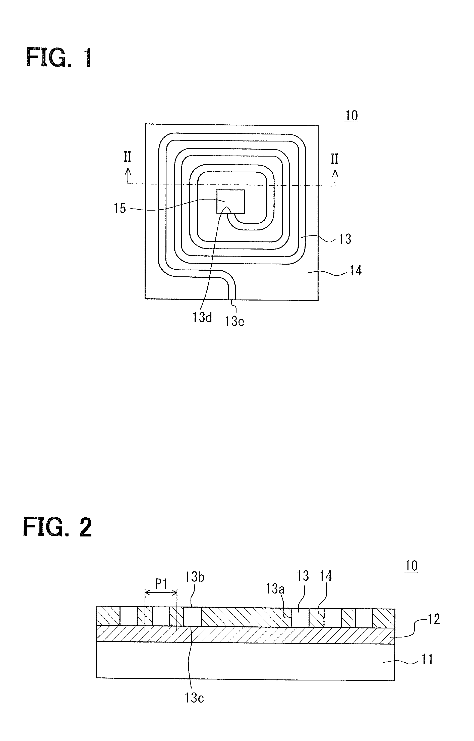
[0037]An optical waveguide sensor 10 according to a first embodiment of the present invention will be described with reference to FIG. 1 and FIG. 2.

[0038]The optical waveguide sensor 10 includes a substrate 11 and an optical waveguide formed above the substrate 11. The optical waveguide includes a core 13 and a lateral clad 14. The core 13 extends in a spiral shape above a surface of the substrate 11. The core 13 and the lateral clad 14 are located in the same layer above the surface of the substrate 11. The lateral clad 14 is in contact with either side surfaces 13a of the core 13, and the core 13 is disposed between the lateral clad 14. The core 13 has an upper surface 13b on an opposite side from the substrate 11. A part of the upper surface 13b provides a transmission surface from which an evanescent wave (evanescent light) leaks and is absorbed by a detected object. In the following description, a thickness direction of the substrate 11, that is, a direction perpendicular to th...

second embodiment

[0057]An optical waveguide sensor 10 according to a second embodiment of the present invention will be described with reference to FIG. 4. In the optical waveguide sensor 10 according to the present embodiment, the upper surface 13b and the lower surface 13c of the core 13 function as transmission surfaces. Furthermore, the optical waveguide sensor 10 includes a support layer 16 that restricts buckling of a membrane MEM.

[0058]The optical waveguide sensor 10 shown in FIG. 4 includes a substrate 11 having an upper surface 11a above which a core 13 and a lateral clad 14 are disposed. The substrate 11 has a removed section 17 that opens on the upper surface 11a. Thus, portions of the core 13 and the lateral clad 14 bridging the removed section 17 form the membrane MEM. Not only the upper surface 13b but also the lower surface 13c of the core 13c in the membrane MEM can function as the transmission surfaces.

[0059]In the example shown in FIG. 4, the removed section 17 also opens on a lowe...

third embodiment

[0071]The inventors studied about more preferred configuration in the configurations described in the first embodiment and the second embodiment with simulation. An optical waveguide according to a third embodiment of the present invention is based on the simulation result. In the following simulation, an optical waveguide sensor 10 in which both an upper surface 13b and a lower surface 13c of a core 13 are exposed surfaces as shown in FIG. 8 is used as a model.

[0072]A relationship between a refractive index of the core 13 and a refractive index of a lateral clad 14 according to the present embodiment will be described below. The refractive index of the core 13 is indicated by n1, the refractive index of the lateral clad 14 is indicated by n2 (1), and a difference in refractive index between the core 13 and the lateral clad 13 is indicated by Δn (=n1−n2).

[0073]In FIG. 9, a relationship between the refractive index difference and a normalized transmittivity is shown in a case where a...


PUM


Abstract

An optical waveguide sensor includes a substrate and an optical waveguide. The optical waveguide includes a core and a lateral clad. The core extends in a spiral shape above a surface of the substrate. The lateral clad is disposed in a same layer as the core above the surface of the substrate and is in contact with either side surfaces of the core. At least a part of a surface of the core located opposite from the substrate is a transmission surface from which light leaks and is absorbed by a detected object.

Description

CROSS REFERENCE TO RELATED APPLICATIONS[0001]The present application is based on and claims priority to Japanese Patent Application No. 2010-103181 filed on Apr. 28, 2010, the contents of which are incorporated in their entirety herein by reference.BACKGROUND OF THE INVENTION[0002]1. Field of the Invention[0003]The present invention relates to an optical waveguide sensor using an evanescent wave that leaks from a core of an optical waveguide. The present invention also relates to a manufacturing method of an optical waveguide sensor.[0004]2. Description of the Related Art[0005]JP-A-2005-61904 discloses an optical waveguide sensor using an evanescent wave that leaks from a core of an optical waveguide.[0006]The optical waveguide sensor is made of a silicon-on-insulator (SOI) substrate. The optical waveguide includes a silicon thin-line core and a clad layer. The silicon thin-line core is formed by processing a silicon layer located on a buried oxide layer in the SOI substrate. The cl...

Claims


Application Information

Patent Timeline
IPC IPC(8): G02B6/02B05D5/06
CPCG01N21/552G02B6/125G01N2021/7783
Inventor YAMASHITA, SHUICHITAKEUCHI, YUKIHIRO
Owner DENSO CORP
Why Eureka
Try Eureka