Manufacturing Method of Identifiable Print Circuit Board

a manufacturing method and print circuit board technology, applied in the direction of printed circuit assembling, printed circuit non-printed electric components association, resistive material coating, etc., can solve the problem of inability to obtain the detailed manufacturing record of each print circuit board, inability to use the conventional manufacturing method in the manufacture of print circuit boards, and high cost of conventional manufacturing methods. to achieve the effect of effective monitoring of each manufacturing process

Active Publication Date: 2011-11-03
WUS PRINTED CIRCUIT
View PDF2 Cites 4 Cited by
  • Summary
  • Abstract
  • Description
  • Claims
  • Application Information

AI Technical Summary

Benefits of technology

[0010]The primary objective of this invention is to provide a manufacturing method of identifiable print circuit board, with effective monitoring of each manufacturing process of the obtained print circuit board.

Problems solved by technology

Thus, it is impossible for the identifiable number or pattern Z to be further used in obtaining the detailed manufacturing record of each print circuit board 9, especially in the early stages of the manufacturing process, such as piling and laminating.
Yet, due to the high cost for the laser machine, the cost of the conventional manufacture method will be significantly high if the laser processing step is frequently carried out by forming the identifiable number or pattern Z on each print circuit board 9 in each manufacturing step.
Additionally, although the art of Radio Frequency Identification (RFID) has been widely put to use in each field of remote identification, it is still unable to be used in manufacture of print circuit board because of the poor tolerance of the RFID chip to high temperature and pressure.

Method used


Image

  • Manufacturing Method of Identifiable Print Circuit Board
  • Manufacturing Method of Identifiable Print Circuit Board
  • Manufacturing Method of Identifiable Print Circuit Board

Examples


Embodiment Construction

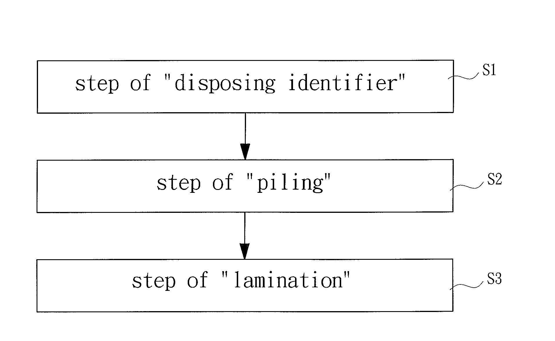
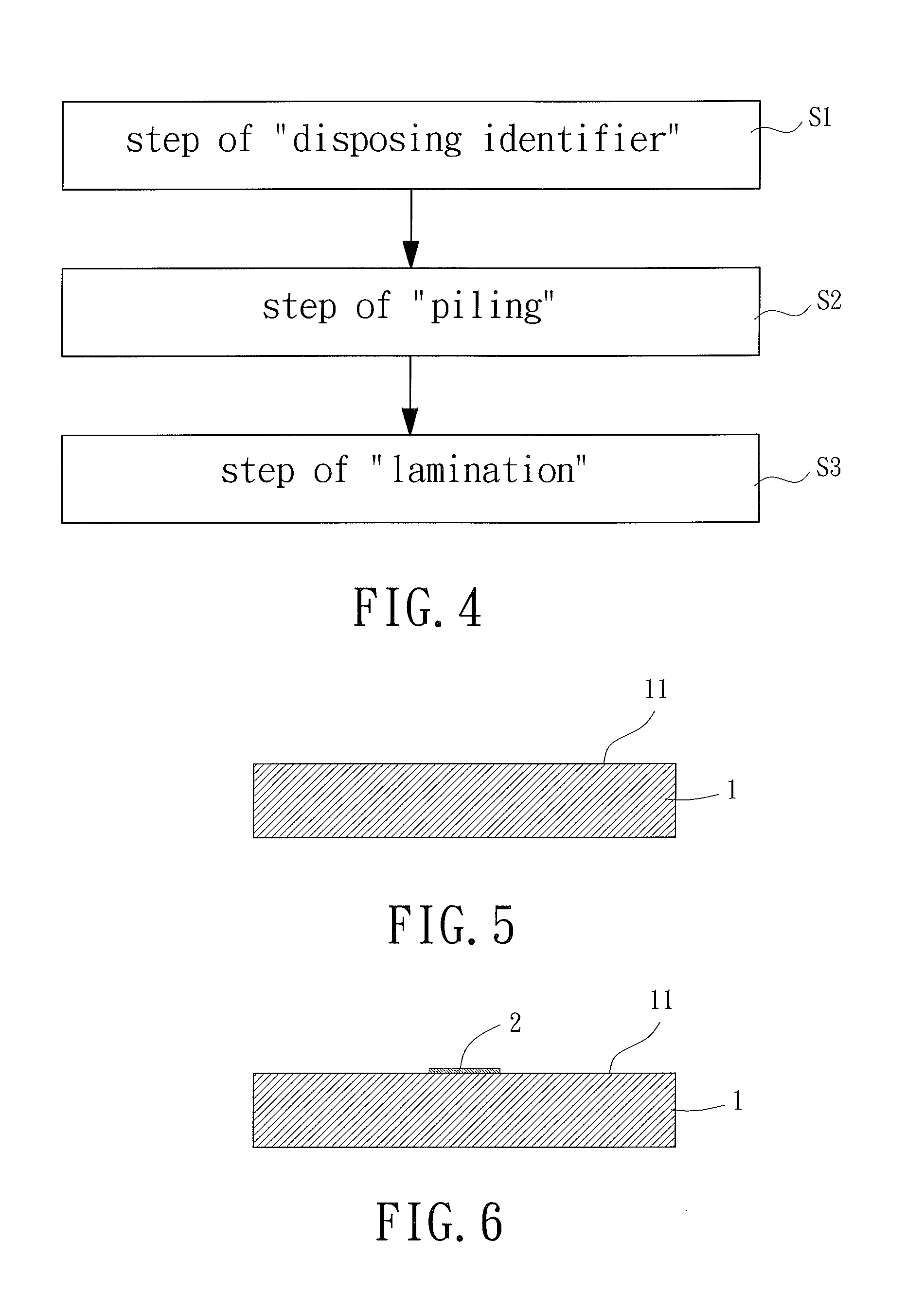
[0027]Referring to FIG. 4, a manufacturing method of identifiable print circuit board comprises a step of “disposing identifier S1”, a step of “piling S2”, and a step of “lamination S3”.

[0028]With reference to FIGS. 5 and 6, in the step of “disposing identifier S1” of a preferable embodiment of the present invention, a base plate 1 with a surface 11 being defined as a manufacturing surface, and a primary identifier 2 are provided, wherein the primary identifier 2 is disposed on the manufacturing surface of the base plate 1. More specifically, the base plate 1 of the present embodiment is made of copper clad laminate (CCL) but is not limited as it may be made of any material that is adapted for use. The primary identifier 2 can be made either by directly printing on the surface 11 of the base plate 1, or by manufacturing into the form of a tab and then sticking the tab on the base plate 1 for recognition. As an example, the primary identifier 2 is manufactured into tab and stuck on t...


PUM

PropertyMeasurementUnit
pressureaaaaaaaaaa
temperatureaaaaaaaaaa
areaaaaaaaaaaa

Abstract

A manufacturing method of identifiable print circuit board comprises a step of “disposing identifier”, by providing a base plate, defining a surface of the base plate as a manufacturing surface, and disposing a primary identifier on the manufacturing surface; a step of “piling”, by sequentially piling up an insulating layer and a circuit layer with a penetrating area on the manufacturing surface, with the penetrating area in alignment with the position of the primary identifier; and a step of “lamination”, by laminating the base plate, the insulating layer, and the circuit layer at a temperature not less than 150° C. and a pressure not less than 280 psi to obtain a print circuit board.

Description

BACKGROUND OF THE INVENTION[0001]1. Field of the Invention[0002]The present invention relates to a manufacturing method of circuit board and, more particularly, to a manufacturing method of identifiable print circuit board.[0003]2. Description of the Related Art[0004]Referring to FIG. 1, a conventional manufacturing method of print circuit board (PCB) is processed by piling up a base plate 91, two thermosetting films 92 and two copper foils 93, with each thermosetting film 92 sandwiched in between the base plate 91 and the copper foils 93; and laminating the base plate 91, the thermosetting films 92 and the copper foils 93 at over 150° C., 280 psi as shown in FIG. 2, so as to obtain a print circuit board 9 with a first layer of circuit (copper foils 93) formed on the base plate 91. Otherwise, if it is necessary, the above lamination can be repeated to repeatedly laminating additional thermosetting films and copper foils on the first layer of circuit (copper foils 93) to form a print...

Claims


Application Information

Patent Timeline
Patent Type & Authority Applications(United States)
IPC IPC(8): H05K3/10
CPCY10T29/49117Y10T29/49124H05K2201/09936Y10T29/49133H05K1/0266Y10T29/49155
Inventor CHEN, CHIH-KANGLIN, TIEN-JENMAI, WEI-JEN
Owner WUS PRINTED CIRCUIT
Why Eureka
Try Eureka