Semiconductor device and method of manufacturing the same

Active Publication Date: 2011-09-29
PANASONIC SEMICON SOLUTIONS CO LTD
View PDF2 Cites 9 Cited by
  • Summary
  • Abstract
  • Description
  • Claims
  • Application Information

AI Technical Summary

Benefits of technology

[0009]In order to prevent the implantation of boron to the source layers 33, a mask may be formed on the source layers 33 during the formation of the body contact layer 38. However, the formation of a mask increases the number of steps of manufacturing the semicon

Problems solved by technology

However, the formation of a mask increases the numbe

Method used


Image

  • Semiconductor device and method of manufacturing the same
  • Semiconductor device and method of manufacturing the same
  • Semiconductor device and method of manufacturing the same

Examples


first embodiment

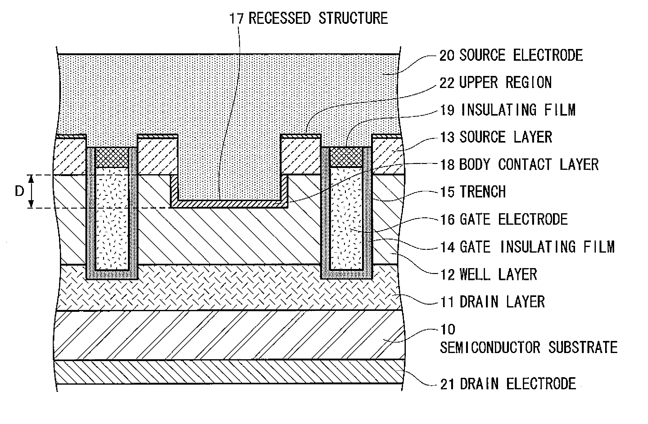
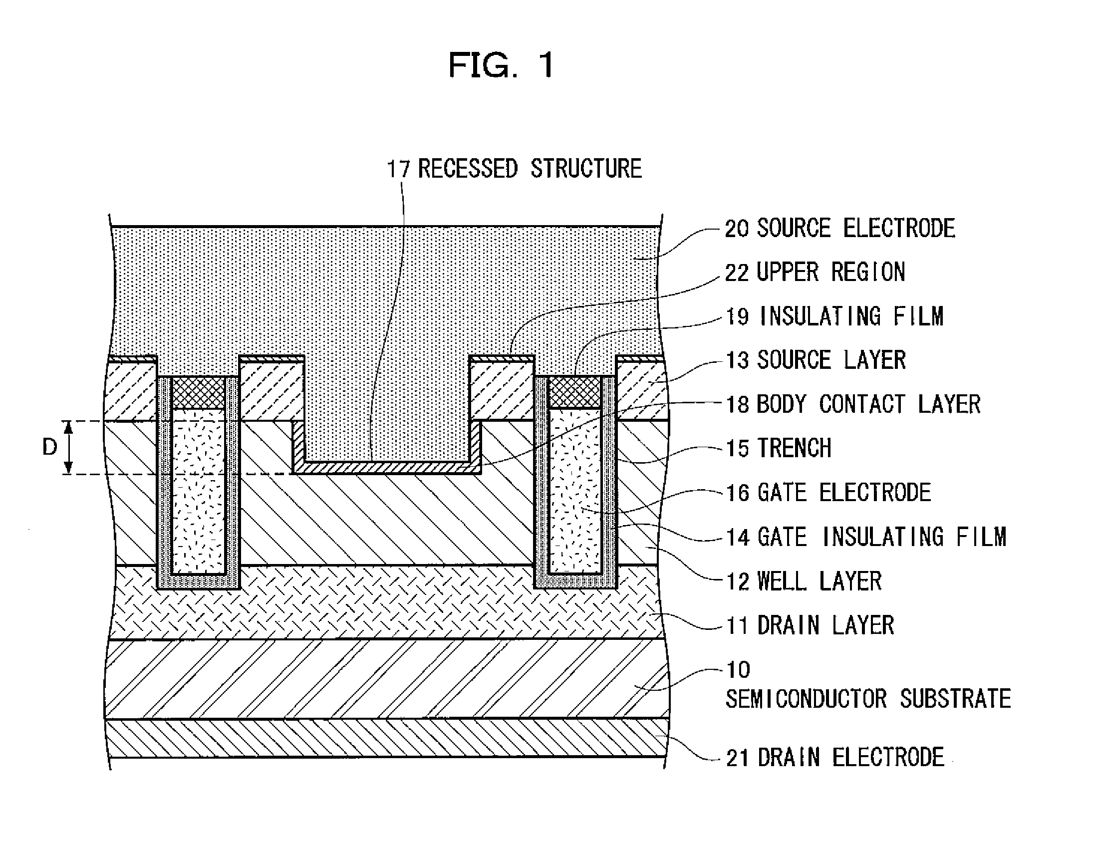
[0037]Referring to FIG. 1, the following will describe a semiconductor device according to a first embodiment.

[0038]FIG. 1 is a sectional view showing the structure of a high-voltage vertical MOSFET according to the first embodiment.

[0039]As shown in FIG. 1, in the high-voltage vertical MOSFET according to the first embodiment, an N-type drain layer 11 is formed on an N-type semiconductor substrate 10 by, e.g., an epitaxial method and a P-type well layer 12 is formed on the surface of the drain layer 11. Further, the P-type well layer 12 has a region serving as a channel region on the front side of the N-type semiconductor substrate 10. Moreover, N-type source layers 13 are selectively formed on the well layer 12 on the front side of the N-type semiconductor substrate 10. Furthermore, trenches 15 are formed in contact with the source layers 13 so as to reach the drain layer 11 from the well layer 12, the inner surfaces of the trenches 15 are covered with gate insulating films 14, an...

second embodiment

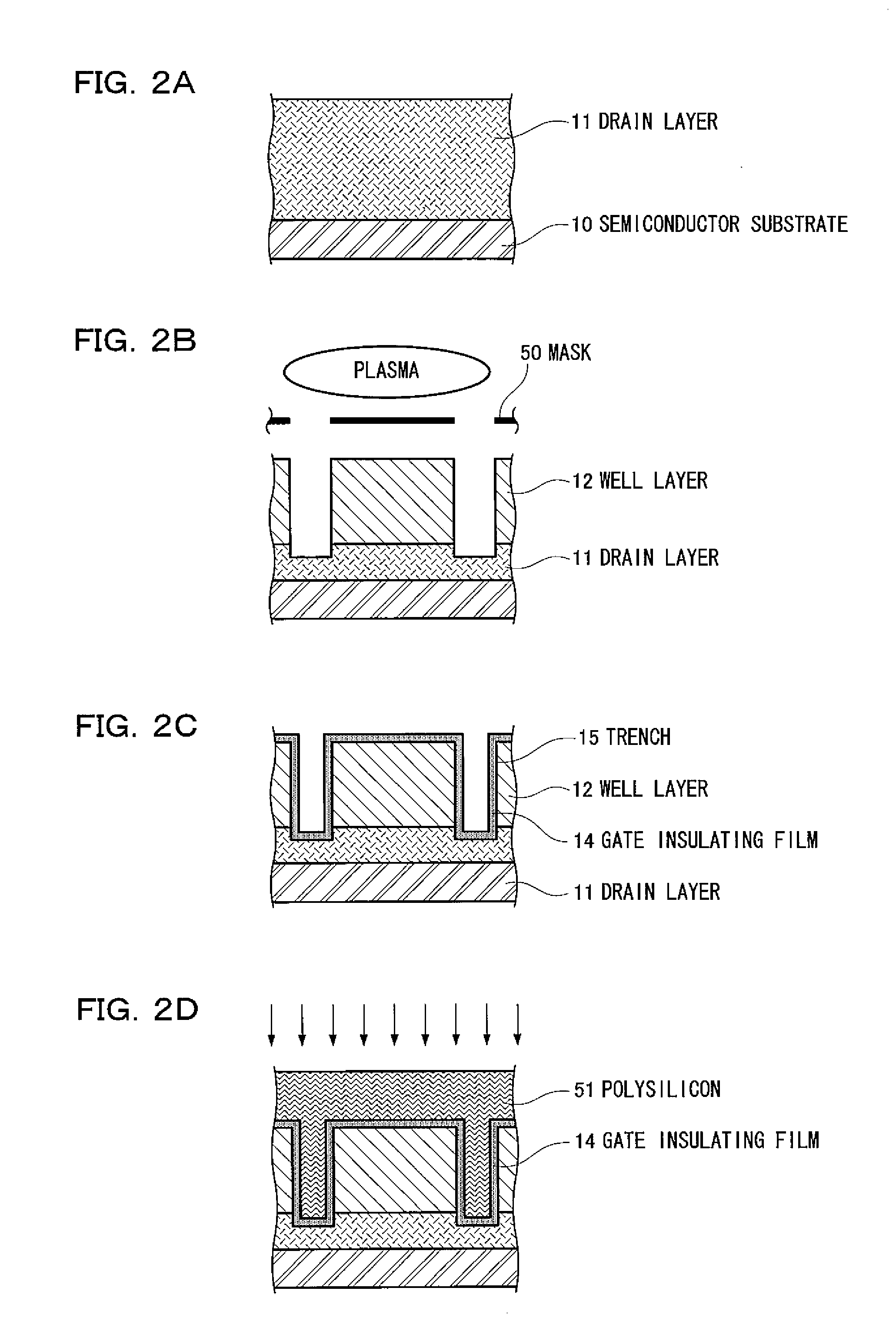
[0063]Referring to FIGS. 7 and 8A to 8C, the following will describe a semiconductor device and a method of manufacturing the same according to a second embodiment.

[0064]FIG. 7 is a sectional view showing the structure of a high-voltage vertical MOSFET according to the second embodiment. The same configurations as FIG. 1 are indicated by the same reference numerals and the explanation thereof is omitted.FIGS. 8A to 8C are process sectional views for explaining the method of manufacturing the semiconductor device according to the second embodiment.

[0065]The semiconductor device and the method of manufacturing the same according to the second embodiment are different from those of the first embodiment as follows: the side of a recessed structure 67 has an inwardly tapered portion 70 that tapers down toward the bottom of the recessed structure 67 and a dopant is not implanted diagonally but only in the vertical direction during the formation of a body contact layer 68.

[0066]As shown in...


PUM


Abstract

A body contact layer 18 is formed on the side of a recessed structure 17 as well as in the bottom of the recessed structure 17, so that a contact area between the body contact layer 18 and a well layer 12 is increased and the amount of dopant implanted to the body contact layer 18 is suppressed.

Description

FIELD OF THE INVENTION[0001]The present invention relates to a semiconductor device and particularly relates to a high-voltage vertical MOSFET and a method of manufacturing the same.BACKGROUND OF THE INVENTION[0002]In vertical MOSFETs used for, e.g., switches of power sources, it has been requested to improve breakdown voltages while reducing on resistances. In a high-voltage vertical MOSFET according to the related art, the parasitic resistances of a body contact layer and a well layer are reduced by increasing the dopant concentrations of the body contact layer and the well layer and the potential of a channel region is stabilized, so that the breakdown voltage is improved.[0003]Referring to FIG. 9, the following will describe the structure of the high-voltage vertical MOSFET according to the related art.[0004]FIG. 9 is a sectional view of the structure of the high-voltage vertical MOSFET according to the related art, showing the structure of a pair of transistors.[0005]As shown i...

Claims


Application Information

Patent Timeline
IPC IPC(8): H01L29/78H01L21/336
CPCH01L21/266H01L29/66666H01L29/7827
Inventor HAMADA, MITSUHIROJOKYU, KATSUYOSHI
Owner PANASONIC SEMICON SOLUTIONS CO LTD
Why Eureka
Try Eureka