Thin film coated process kits for semiconductor manufacturing tools

a technology of process kits and semiconductors, applied in the direction of coatings, chemical vapor deposition coatings, chemical apparatus and processes, etc., can solve the problems of short life of parts, frequent and long conditioning of process chambers, and prone to attack and degradation of materials typically used for process kits

Inactive Publication Date: 2011-08-25
TAIWAN SEMICON MFG CO LTD
View PDF14 Cites 326 Cited by
  • Summary
  • Abstract
  • Description
  • Claims
  • Application Information

AI Technical Summary

Benefits of technology

[0008]In a semiconductor manufacturing plasma etching apparatus including an etching chamber and a process kit formed of quartz, another aspect of the invention is the improvement comprising coating exposed surfaces of the process kit with Y2O3 using at least one of CVD (chemical vapor deposition) and PVD (physical vapor deposition).

Problems solved by technology

The materials typically used for process kits are prone to attack and degradation in fluorine-based chemistries.
Such materials that are prone to attack include quartz, silicon, alumina and anodized parts and as a result, these parts have short lifetimes and require frequent and lengthy conditioning of the process chambers within which they are used.
Quartz, for example, is a favored material for process kits but is subject to erosion and degradation in fluorine-based etching and cleaning chemistries.
As the quartz process kit erodes, it causes particle contamination, it alters the impedance of the chamber and therefore the plasma performance, and it needs to be replaced.
By coating the exposed surfaces of the process kit with materials other than designed by the manufacturer, however, the impedance of the process chamber is undesirably changed and therefore the etch characteristics and cleaning characteristics of the tool are compromised, i.e., process shifting occurs.
Moreover, conventional coatings are subject to cracking, peeling and delamination which produce particle contamination.

Method used


Image

  • Thin film coated process kits for semiconductor manufacturing tools
  • Thin film coated process kits for semiconductor manufacturing tools
  • Thin film coated process kits for semiconductor manufacturing tools

Examples


Embodiment Construction

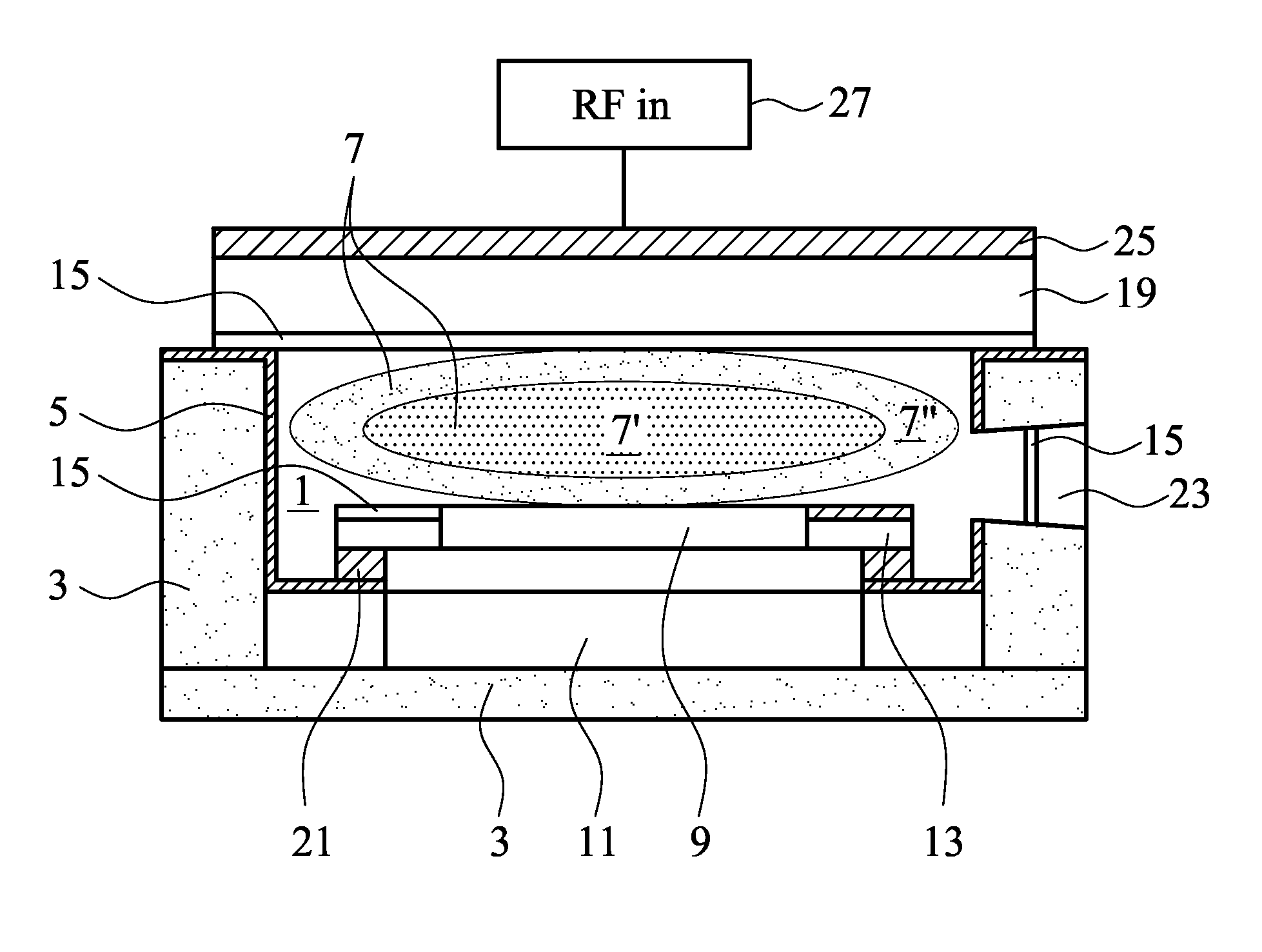
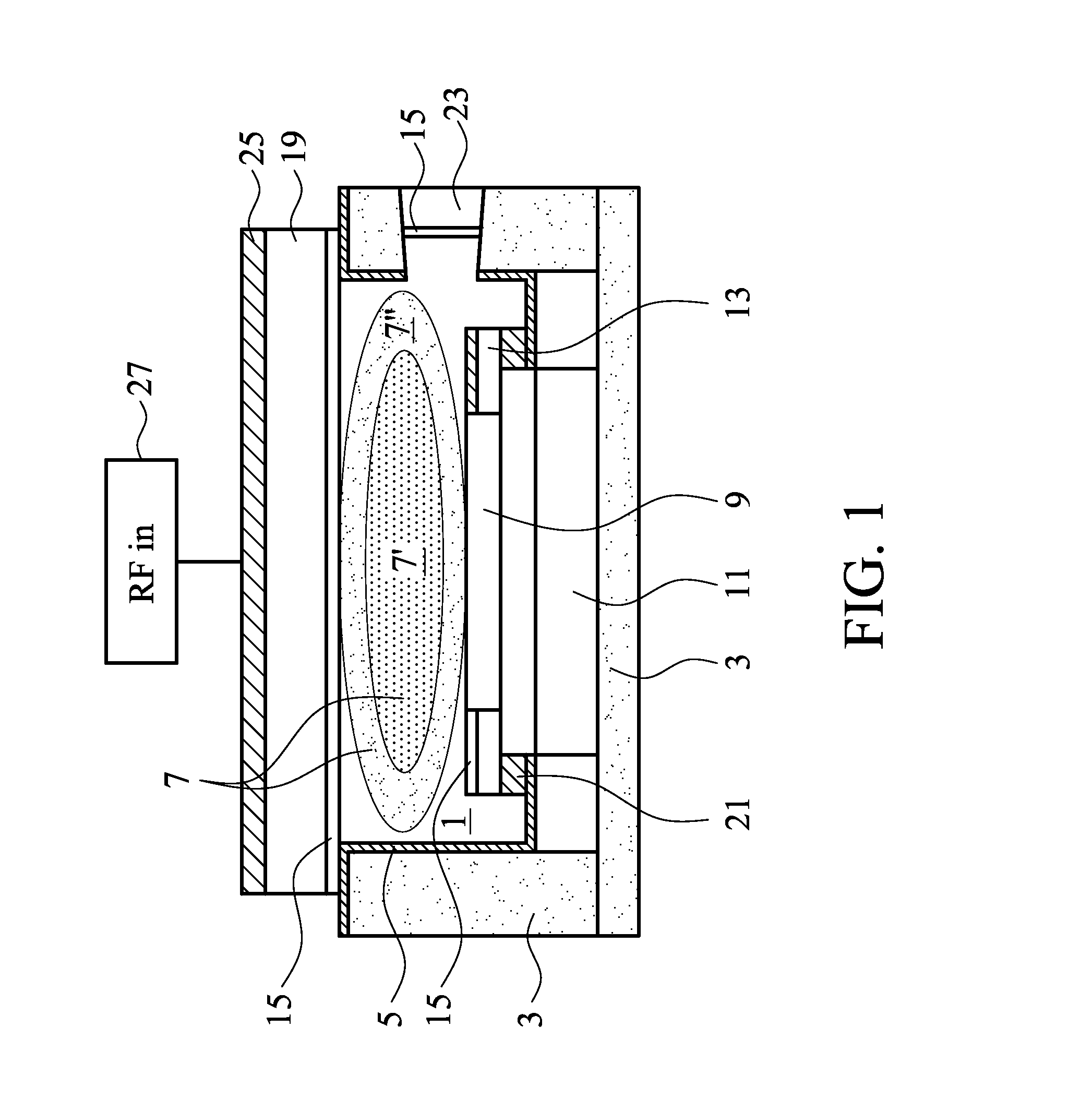
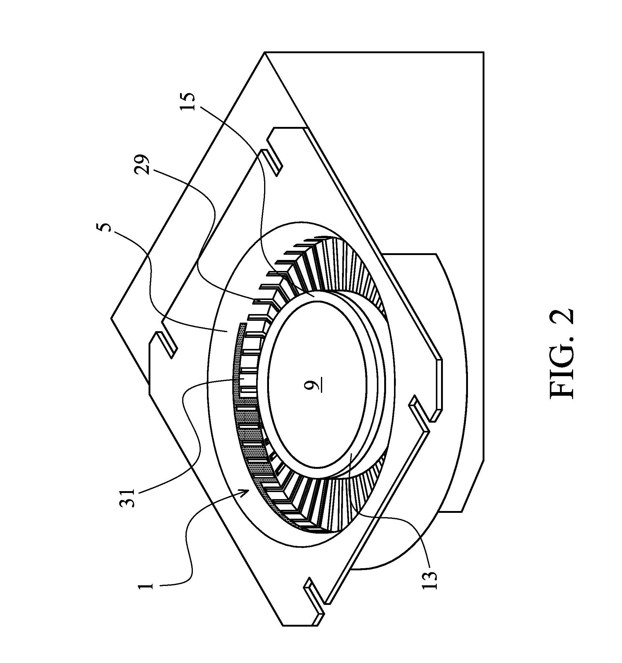
[0013]One aspect of the invention provides for a yttria, Y2O3 coating formed using chemical vapor deposition, CVD, or physical vapor deposition, PVD, on surfaces of a process kit inside a plasma processing chamber that may be used for plasma etching, plasma cleaning, or both. Other suitable thin film deposition processes may be used in other exemplary embodiments. The plasma processing chamber may be a chamber in any of various plasma processing apparatuses made by various manufacturers that are commercially available and used in the semiconductor manufacturing industry. The plasma processing chamber may be a chamber that is primarily used for etching processes or cleaning processes and the processing chamber may be a chamber dedicated to a fluorine-based processing chemistry. As referred to herein, process kit refers to the insulating components of the process chamber apparatus that are capable of reducing or eliminating electrical arcing from exposed metal in the chamber. The proc...


PUM

PropertyMeasurementUnit
thicknessaaaaaaaaaa
thicknessesaaaaaaaaaa
thicknessaaaaaaaaaa

Abstract

A plasma processing apparatus used in semiconductor device manufacturing includes a process kit formed of insulating materials such as quartz and coated with a Y2O3 coating. The Y2O3 coating is a thin film formed using suitable CVD or PVD operations. The Y2O3 coating is resistant to degradation in fluorine etching chemistries commonly used to etch silicon in semiconductor manufacturing. The plasma processing apparatus may be used in etching, stripping and cleaning operations. Also provided in another embodiment is a plasma processing apparatus having a quartz process kit coated with a sapphire-like film.

Description

RELATED APPLICATION[0001]This application is related to and claims priority of U.S. Provisional Application Ser. No. 61 / 308,015 entitled THIN FILM COATED PROCESS KITS FOR SEMICONDUCTOR MANUFACTURING TOOLS, filed Feb. 25, 2010, the contents of which are incorporated herein by reference as if set forth in their entirety.FIELD OF THE INVENTION[0002]The present invention relates, most generally, to semiconductor device manufacturing. More particularly, the present invention relates to semiconductor manufacturing tools and methods and systems for reducing degradation of such tools.BACKGROUND[0003]Plasma etching operations are used very frequently in the rapidly advancing art of semiconductor device manufacturing. Various processing operations involve RIE (reactive ion etching) or other plasma etching operations to etch materials formed on a semiconductor device, typically to create a pattern in a material layer formed on a semiconductor substrate. Plasma cleaning operations are also comm...

Claims


Application Information

Patent Timeline
Patent Type & Authority Applications(United States)
IPC IPC(8): H01L21/465C23C16/44C23C16/06
CPCH01J37/32477H01J37/32495H01J37/32642H01J37/32633H01J37/32623
Inventor LIU, HSU-SHUIWANG, YEH-CHIEHPAI, JIUN-RONG
Owner TAIWAN SEMICON MFG CO LTD
Why Eureka
Try Eureka