
Chip-scale atomic clock with two thermal zones

a technology of atomic clocks and thermal zones, applied in the field of chip-scale atomic clocks with two thermal zones, can solve the problems of temperature sensitivity of csacs that can still be a problem, csacs become inaccurate, and components to change the temperatur

Active Publication Date: 2011-08-04
HONEYWELL INT INC
View PDF7 Cites 18 Cited by
  • Summary
  • Abstract
  • Description
  • Claims
  • Application Information

AI Technical Summary

Benefits of technology

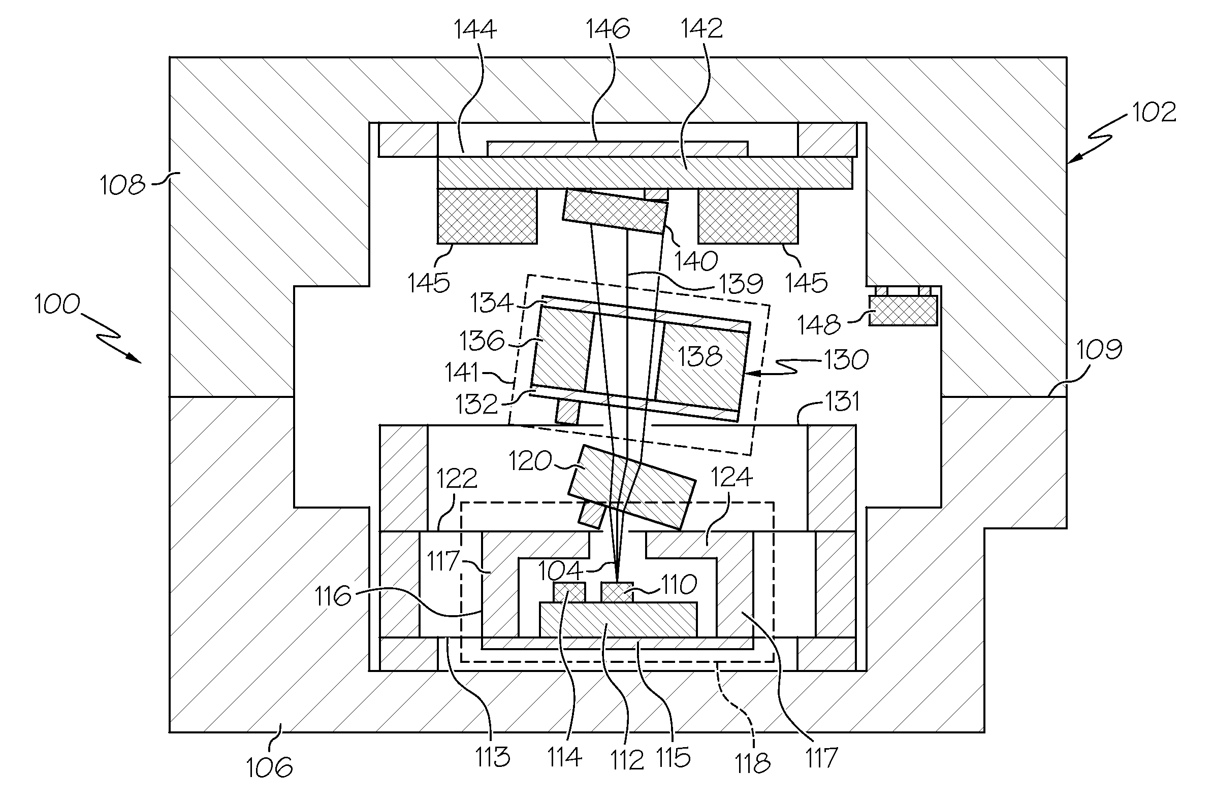
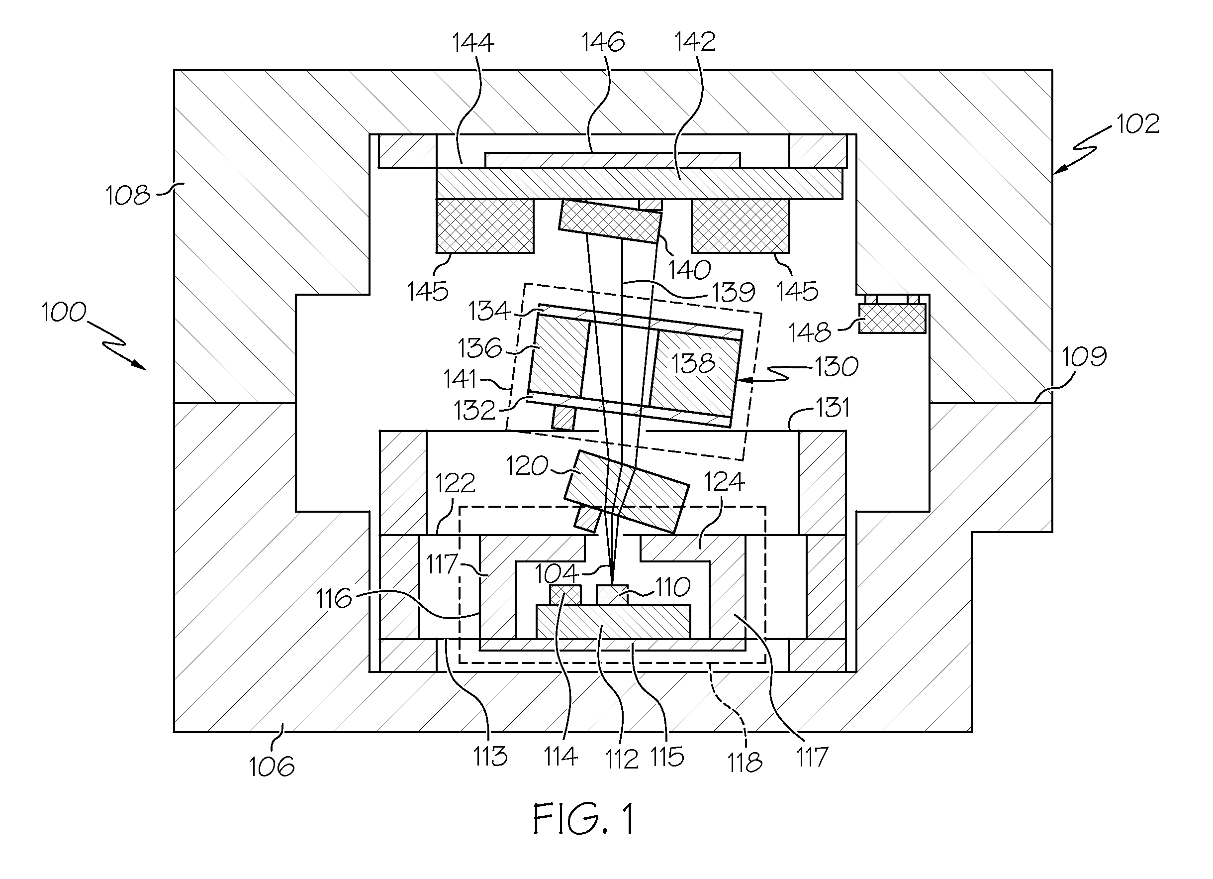
[0007]A chip-scale atomic clock comprises a physics package and a laser die located in a first thermal zone of the physics package. A quarter wave plate is mounted in the physics package and is in optical communication with the laser die. A vapor cell is mounted in the physics package and is in optical communication with the quarter wave plate. The vapor cell is located in a second thermal zone th

Problems solved by technology

It is known that some CSACs become inaccurate when the ambient temperature changes.
This is due in part to the fact that two of the components in the CSAC, the vapor cell and the VCSEL, are not operated at their most stable temperatures.
One of the more challenging aspects of making CSACs for military applications involves dealing with the temperature variations that real military systems encounter during use.
Even though attempts have been made to stabilize the temperature of the most sensitive components, the temperature sensitivity of the CSACs can still be a problem.
For example, radiative coupling and gas-phase thermal conduction from the components inside the physics package to the walls of the package can cause the temperature of those components to change.

Method used


Image

  • Chip-scale atomic clock with two thermal zones
  • Chip-scale atomic clock with two thermal zones
  • Chip-scale atomic clock with two thermal zones

Examples


Embodiment Construction

[0014]In the following detailed description, embodiments are described in sufficient detail to enable those skilled in the art to practice the invention. It is to be understood that other embodiments may be utilized without departing from the scope of the invention. The following detailed description is, therefore, not to be taken in a limiting sense.

[0015]A chip-scale atomic clock (CSAC) is provided that has a two-thermal zone configuration, including a first thermal zone for a laser die, such as a vertical-cavity surface-emitting laser (VCSEL), and a second thermal zone for a vapor cell, in the CSAC. The first thermal zone provides a first operation temperature at a first stability point associated with the laser die, and the second thermal zone provides a second operation temperature at a second stability point associated with the vapor cell.

[0016]The two-thermal zone configuration of the chip-scale atomic clock allows the vapor cell and laser die to be operated at their most sta...


PUM


Abstract

A chip-scale atomic clock comprises a physics package and a laser die located in a first thermal zone of the physics package. A quarter wave plate is mounted in the physics package and is in optical communication with the laser die. A vapor cell is mounted in the physics package and is in optical communication with the quarter wave plate. The vapor cell is located in a second thermal zone that is independent from the first thermal zone. An optical detector is mounted in the physics package and is in optical communication with the vapor cell. The first thermal zone provides a first operation temperature at a first stability point associated with the laser die, and the second thermal zone provides a second operation temperature at a second stability point associated with the vapor cell.

Description

CROSS-REFERENCE TO RELATED APPLICATION[0001]This application claims the benefit of U.S. Provisional Patent Application Ser. No. 61 / 301,497, filed on Feb. 4, 2010, which is incorporated herein by reference.GOVERNMENT LICENSE RIGHTS[0002]The U.S. Government may have certain rights in the present invention as provided for by the terms of Government Contract prime number FA8650-01-C-1125 with the U.S. Air Force.BACKGROUND[0003]Chip-Scale Atomic Clocks (CSACs) contain vapors of alkali metals, typically either rubidium (Rb) or cesium (Cs), which are located in vapor cells. The walls of the vapor cells are typically made from glass and silicon. A bichromatic (2 wavelength) optical field is sent through the vapor, exciting hyperfine transitions using a phenomenon called coherent population trapping. A rubidium-based CSAC, for example, works by exciting the D1 hyperfine transition using a vertical-cavity surface-emitting laser (VCSEL) that is tuned to the broad absorption at 795 nm and radio...

Claims


Application Information

Patent Timeline
IPC IPC(8): H03B17/00
CPCG04F5/145H01S5/005H01S5/183H01S5/024H01S5/02296H01S5/02H01S5/02208H01S5/02453H01S5/02476H01S5/02257
Inventor YOUNGNER, DANIEL W.RIDLEY, JEFF A.SALIT, MARY K.LU, SON T.
Owner HONEYWELL INT INC
Learn More