Shallow trench isolation structure having air gap, CMOS image sensor using the same and method of manufacturing CMOS image sensor

a technology of isolation structure and air gap, which is applied in the direction of diodes, semiconductor devices, radio frequency controlled devices, etc., can solve the problems of locos technology not being applicable and the limitation of isolation layer width to reduce the width, so as to suppress the generation of dark current, suppress the diffusion of electrons, and achieve high-quality images

Active Publication Date: 2011-08-04
INTELLECTUAL VENTURES II
View PDF14 Cites 28 Cited by
  • Summary
  • Abstract
  • Description
  • Claims
  • Application Information

AI Technical Summary

Benefits of technology

[0028]According to the CMOS image sensor of the present invention, the shallow trench isolation structure has the air gap to suppress photons injected from neighboring pixels and to suppress the generation of dark current, so a high quality image can be achieved.
[0029]In addition, impurities are removed

Problems solved by technology

However, according to the LOCOS technology, an oxide layer is formed in a region where a lateral diffusion is not required, so that there is limitation to reduce the width

Method used


Image

  • Shallow trench isolation structure having air gap, CMOS image sensor using the same and method of manufacturing CMOS image sensor
  • Shallow trench isolation structure having air gap, CMOS image sensor using the same and method of manufacturing CMOS image sensor
  • Shallow trench isolation structure having air gap, CMOS image sensor using the same and method of manufacturing CMOS image sensor

Examples


Embodiment Construction

Technical Problem

[0007]Accordingly, the present invention has been made to solve the above-mentioned problems occurring in the prior art, and an object of the present invention is to provide a shallow trench isolation structure capable of preventing degradation of the optical device characteristics caused by high integration of optical devices.

[0008]Another object of the present invention is to provide a CMOS image sensor having such a shallow trench isolation structure and a method of manufacturing the same.

Technical Solution

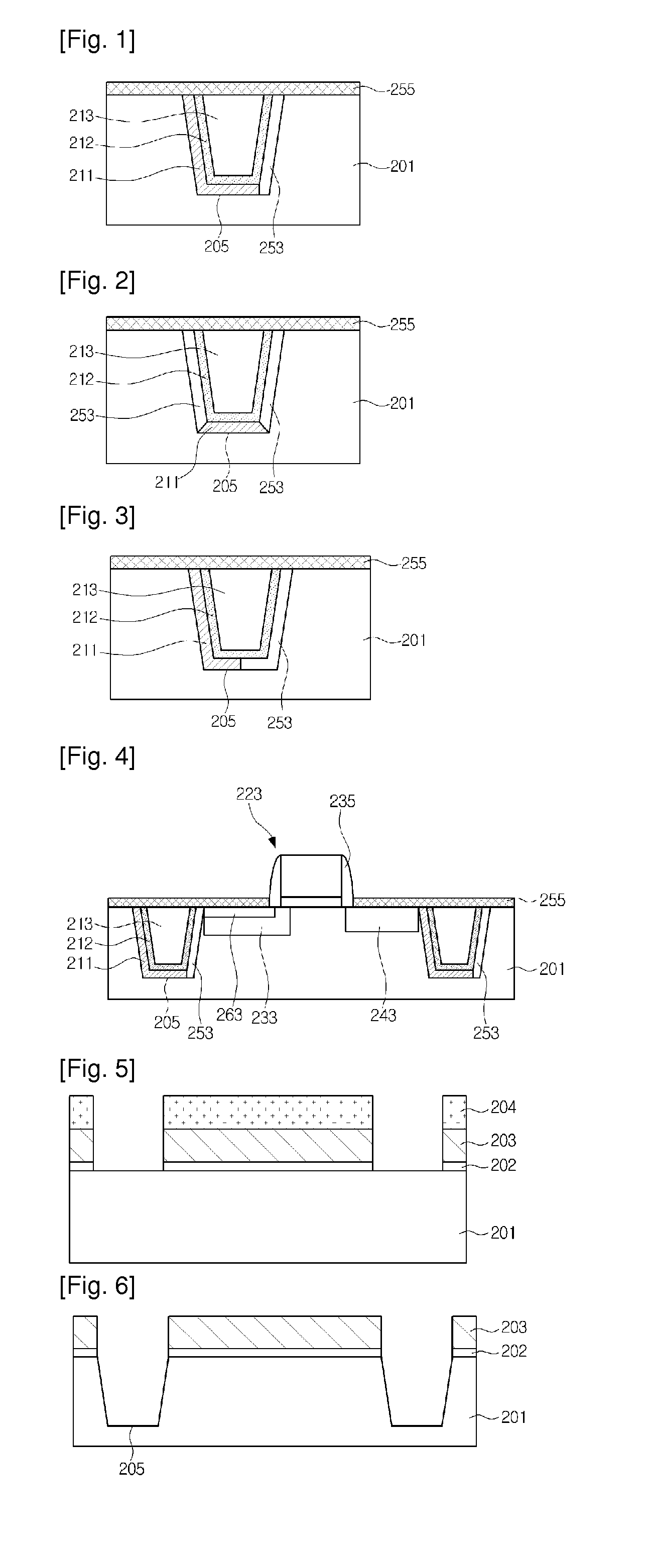
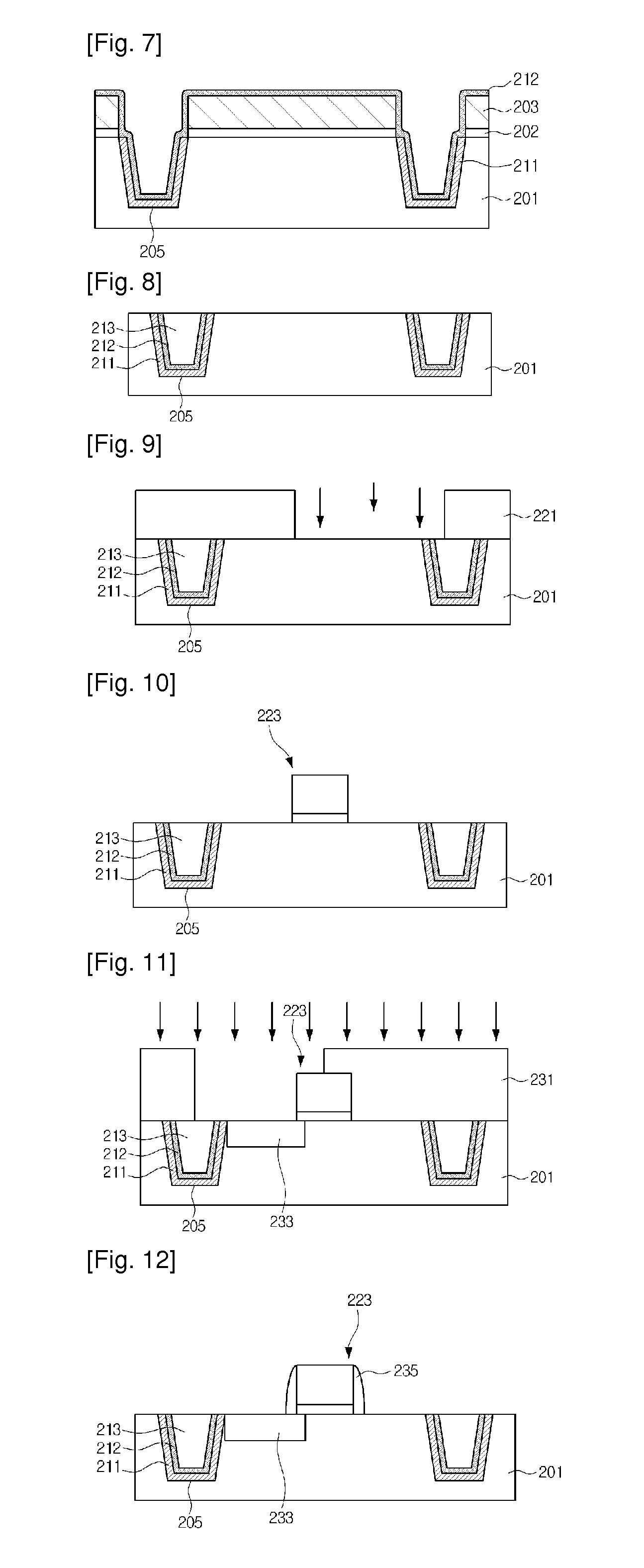
[0009]In accordance with an aspect of the present invention, there is provided a shallow trench isolation structure comprising: a trench formed on an inactive region of a substrate; an inner wall oxide layer formed on the trench; a liner formed on the inner wall oxide layer; an oxide layer formed on the liner to fill the trench; an air gap formed between the trench and the liner; and a buffer layer to seal the air gap.

[0010]The air gap may be formed at one late...


PUM


Abstract

Disclosed is a shallow trench isolation structure having an air gap for suppressing the dark currents and cross-talk which occur in CMOS image sensors. The shallow trench isolation structure suppresses photons injected from neighboring pixels and dark current, so that high-quality images are obtained. Since impurities are removed from a p type ion implantation region for a photodiode when an inner wall oxide layer is etched to form the air gap, the p type ion implantation region has a uniform doping profile, thereby suppressing the diffusion of electrons towards the surface and achieving an image having a high quality.

Description

TECHNICAL FIELD[0001]The present invention relates to a semiconductor device, such as a CMOS sensor. More particularly, the present invention relates to a shallow trench isolation structure having an air gap, a CMOS image sensor using the same, and a method of manufacturing the CMOS sensor.BACKGROUND ART[0002]With the development of semiconductor manufacturing technology, the application fields for semiconductor devices have increased, so various studies and research have been extensively performed to increase the integration degree of the semiconductor devices. As the integration degree of semiconductor devices has increased, studies have been increasingly pursued to fabricate semiconductor devices in a micro-size based on micro-fabrication processes. In micro-fabrication technology for semiconductor devices, isolation layer diminishing technology for isolating devices from each other to integrate devices is very important.[0003]As a conventional isolation technology, the LOCOS (lo...

Claims


Application Information

Patent Timeline
IPC IPC(8): H01L29/06H01L21/762H01L31/18H01L27/146
CPCH01L21/76224H01L21/764H01L27/14689H01L27/1463H01L27/14643H01L21/823481H01L21/76
Inventor SUNG, NAG KYUN
Owner INTELLECTUAL VENTURES II
Why Eureka
Try Eureka