Eureka AIR delivers breakthrough ideas for toughest innovation challenges, trusted by R&D personnel around the world.

Thin film solar cell with ceramic handling layer

a solar cell and ceramic technology, applied in the field of solar cells, can solve the problems of affecting the cost of solar cells formed and packaged in standard wafers, affecting the cost of solar cells, and crystalline silicon still constitutes a significant part of the overall cost, so as to reduce the cost of solar energy production

Active Publication Date: 2011-08-04
SVAGOS TECHNICK INC
View PDF46 Cites 26 Cited by
  • Summary
  • Abstract
  • Description
  • Claims
  • Application Information

AI Technical Summary

Benefits of technology

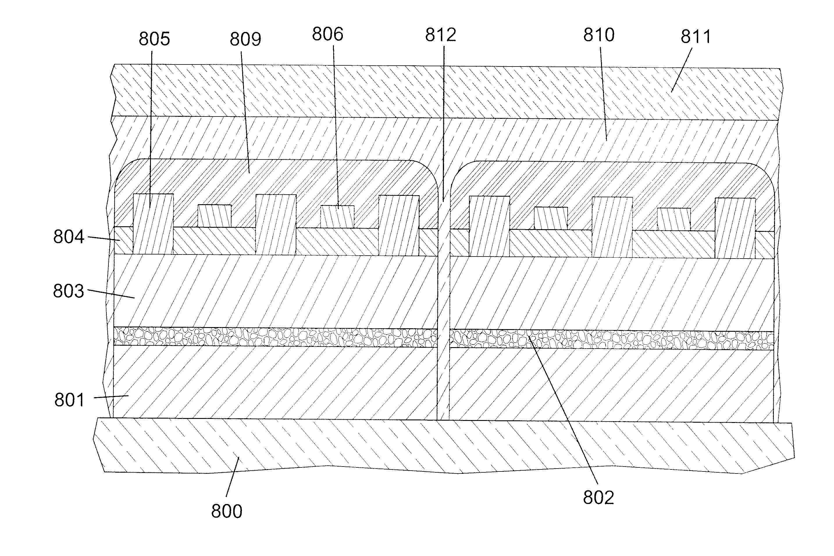
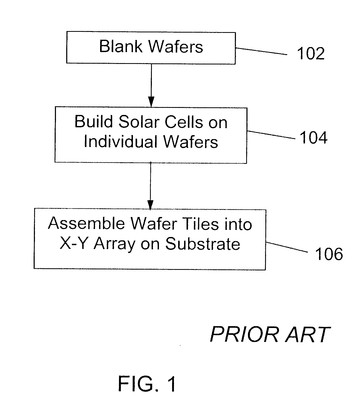
[0009]The present invention turns the prior art strategy on its head, starting with the solar panel and rethinking the unit manufacturing steps in panel size, starting from the surface treatment of the source wafers through to module encapsulation, completely eliminating the need for handling individual thin epitaxial silicon cells. According to one aspect of the invention, the manufacturing sequence is reversed from the conventional prior art sequence. In this aspect of the invention, multiple source wafer tiles are bonded to a support prior to the formation of individual cells, thereby enabling the use of large-scale processing for solar cell fabrication, instead of the wafer-by-wafer approach previously used. This rethinking involves key innovations that make these unit processes robust and reliable. This approach has been enabled by some key innovations described in this invention. This essentially fulfills the vision for the 2020 module, where “Cell and module manufacturing is based on process steps applied to whole panels instead of individual cells” articulated by G. Beaucarne et al. at the 21st European PVEC Conference in 2006. More importantly, panel size semiconductor processing enables a significant reduction in the cost of solar energy production.

Problems solved by technology

Such silicon wafers are relatively expensive and thus severely impact the costs of solar cells in formed and packaged in the standard wafers.
The cost of crystalline silicon still constitutes a significant part of the overall cost, as measured by many of the metrics used to characterize the cost of crystalline solar technology.
It has been difficult or impossible to attain very thin solar cells using the prior art process in which individual PC cells are formed prior to assembly into the final X-Y array needed for a completed solar panel.
Despite the great potential of this prior art method for producing relatively inexpensive, highly efficient solar cells, the method has eluded commercial success for at least three main reasons: (1) some of the unit processes are deficient and difficult to reproduce especially for thin epitaxial wafers; (2) manufacturing strategy generally starts and ends with making individual wafer-size solar cells and, thereafter, assembling them into solar panels; and (3) thin cells break easily, and their economical processing awaits the development of new tools and equipment.

Method used


Image

  • Thin film solar cell with ceramic handling layer
  • Thin film solar cell with ceramic handling layer
  • Thin film solar cell with ceramic handling layer

Examples


embodiment 1

Attachment of the Wafers Prior to Formation of the Porous Layer, with the Use of Thin Film Contacts

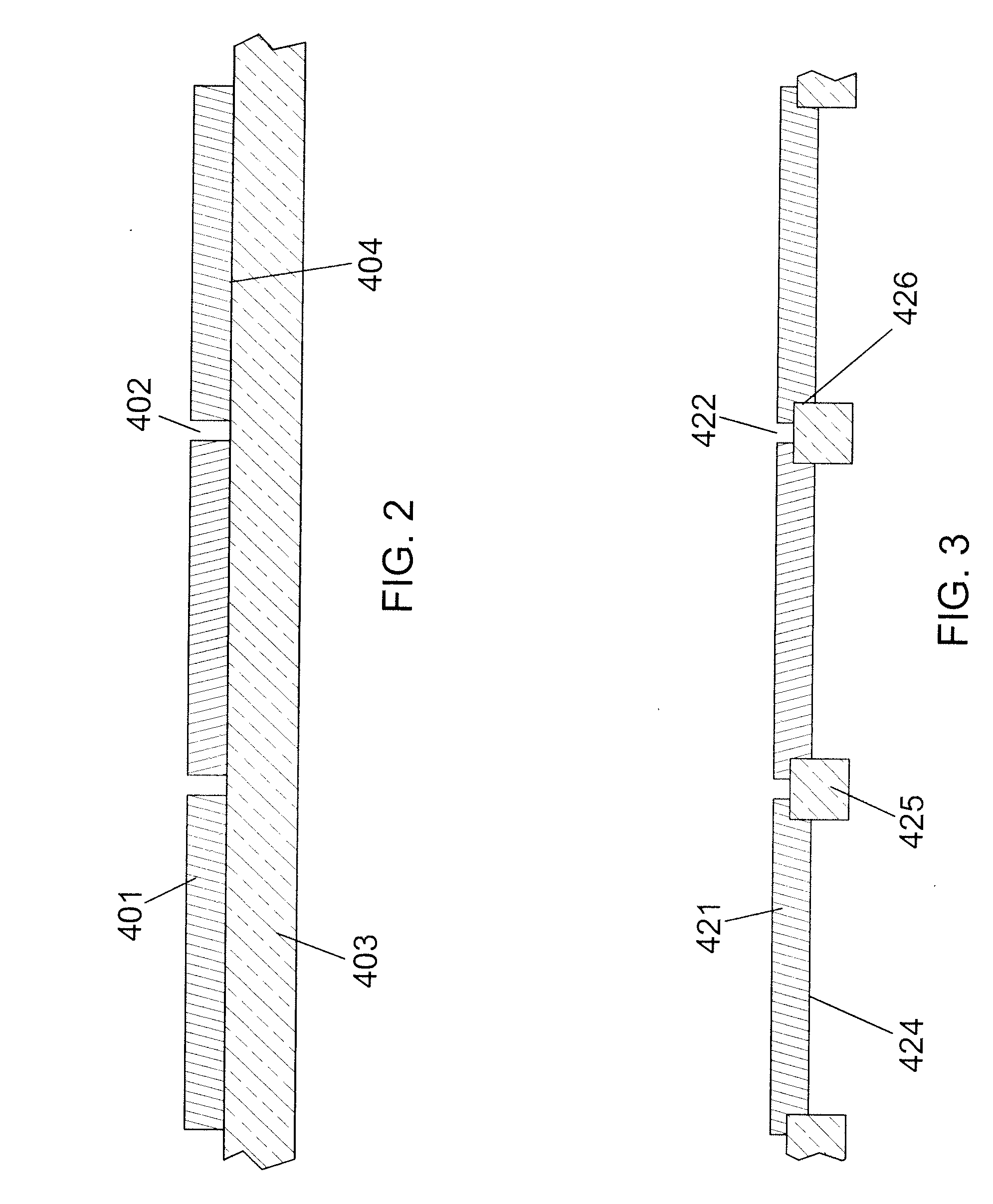
[0121]The flow chart of FIG. 20 illustrates a first embodiment of the first part of a manufacturing process for solar panels. In this process, in step 201, a number of mother wafers are attached to a susceptor, as described in FIGS. 2-4 above. The number of mother wafers may correspond to the full number of PV wafers in a solar panel or a fraction of the full number. Next, in step 202, porous silicon layers are formed on the surfaces of all the mother wafers using an anodization system such as that shown in FIGS. 5 and 6. One or more susceptors are then mounted into a wafer sleeve as shown in FIG. 8, which is designed to interface with an epitaxial reactor such as that described in U.S. patent application Ser. No. 12 / 392,448.

[0122]In step 203, the wafer sleeve comprising one or more susceptors loaded with mother wafers is heated to thermally smooth the surfaces of the porous silicon la...

embodiment 2

Attachment of the Wafers Prior to Formation of the Porous Layer with the Use of Thick Film Contacts

[0126]The flow chart of FIG. 21 illustrates a second embodiment of the first part of a manufacturing process for solar panels. In this process, in step 221, a number of mother wafers are attached to a susceptor, as described above for FIGS. 2-4. The number of mother wafers may correspond to the full number of PV wafers in a solar panel or a fraction of the full number. Next, in step 222, porous silicon layers are formed on the surfaces of all the mother wafers using an anodization system such as that shown in FIGS. 5 and 6. One or more susceptors are then assembled into a wafer sleeve as shown in FIG. 8, which is designed to interface with an epitaxial reactor such as that described in U.S. patent application Ser. No. 12 / 392,448.

[0127]In step 223, the wafer sleeve comprising one or more susceptors loaded with mother wafers is then heated to thermally smooth the surfaces of the porous s...

embodiment 3

Attachment of the Wafers after the Formation of Porous Layers on Each Wafer with the Use of Thin Film Contacts

[0131]The flow chart of FIG. 21 illustrates a third embodiment of the first part of a manufacturing process for solar panels. In this process, in step 241, porous silicon layers are first formatted on the surfaces of each individual mother wafer using an anodization system such as that shown in FIG. 7. Next, a number of mother wafers are attached to a susceptor in step 242, as described above for FIGS. 2-4. The number of mother wafers may correspond to the full number of PV wafers in a solar panel or a fraction of the full number. One or more susceptors are then assembled into a wafer sleeve as shown in FIG. 8, which is designed to operate in an epitaxial reactor. The wafer sleeve comprising one or more susceptors loaded with mother wafers is then heated in step 243 to thermally smooth the surfaces of the porous silicon layers. This thermal smoothing process provides a suffi...


PUM

PropertyMeasurementUnit
Fractionaaaaaaaaaa
Fractionaaaaaaaaaa
Thicknessaaaaaaaaaa

Abstract

A method for fabricating a photovoltaic (PV) cell panel wherein all PV cells are formed simultaneously on a two-dimensional array of monocrystalline silicon mother wafers affixed to a susceptor is disclosed. Porous silicon separation layers are anodized in the surfaces of the mother wafers. The porous film is then smoothed to form a suitable surface for epitaxial film growth. An epitaxial reactor is used to grow n- and p-type films forming the PV cell structures. A glass / ceramic handling layer is then formed on the PV cell structures. The PV cell structures with handling layers are then exfoliated from the mother wafer. The array of mother wafers may be reused multiple times, thereby reducing materials costs for the completed solar panels. The glass / ceramic handling layers provide structural integrity to the thin epitaxial solar cells during the separation process and subsequent handling.

Description

CROSS-REFERENCE TO RELATED APPLICATIONS[0001]This application is a continuation-in-part of U.S. patent application Ser. No. 12 / 399,248 filed Mar. 6, 2009, which claims the benefit of U.S. Provisional Patent Application Ser. No. 61 / 068,629, filed Mar. 8, 2008. The foregoing disclosures are incorporated herein by reference.FIELD OF THE INVENTION[0002]This invention relates generally to solar cells, and more particularly to solar cells with ceramic handling layers, and methods and systems for fabricating said solar cells with ceramic handling layers.BACKGROUND OF THE INVENTION[0003]Silicon is the basic ingredient of many solar cell technologies ranging from thin film amorphous silicon solar cells to single-crystal silicon wafer-based solar cells. High efficiency solar cells start with electronic grade polysilicon grown by chemical vapor deposition. The polysilicon is melted and ingots are pulled from the melt in the Czochralski process and often zone refined to produce silicon ingots o...

Claims


Application Information

Patent Timeline
IPC IPC(8): H01L31/0236H01L31/18
CPCH01L31/02168C03C8/14H01L31/0236H01L31/028H01L31/048H01L31/072H01L31/0725H01L31/0747H01L31/1804H01L31/1896Y02E10/547H01L31/02167C03C3/091C03C3/097C03C8/08H01L31/022425H01L31/02363H01L31/0682Y02E10/546Y02P70/50
Inventor KUMAR, ANANDA H.RAVI, TIRUNELVELI S.GOPAL, VIDYUT
Owner SVAGOS TECHNICK INC
Why Eureka
Eureka Blog
Learn More