
Resistance-based memory with reduced voltage input/output device

Active Publication Date: 2011-07-21
QUALCOMM INC +1
View PDF12 Cites 15 Cited by
  • Summary
  • Abstract
  • Description
  • Claims
  • Application Information

AI Technical Summary

Benefits of technology

[0004]Sensing margin is improved by using an input and output (I / O) transistor device as a sense amplifier load device under core voltage conditions. The increased size of the I / O load device reduces the effects of process variations on threshold voltage, which in turn reduces a variation of sensing margin to improve a mean−3σ noise margin for a device. A threshold voltage of the I / O load devices can be reduced for low-voltage operation by ion implantation, body bias effects, or a combination of both.
[0009]One particular advantage provided by embodiments disclosed herein enables accurate reading of stored data values. By increasing the sensing margin of a memory device, data may be read from the memory device with fewer read errors that may result when the sensing margin is too small to differentiate high and low data values. By reducing variation of the sensing margin of data storage elements in memory devices resulting from process variations, device yield can be improved and manufacturing costs can be reduced.
[0010]Another particular advantage provided by embodiments disclosed herein provides more accurate reading of data values enabled by using input and output (I / O) transistors operating at a lower supply voltage than at which I / O transistors usually operate. Using I / O transistors, even at a reduced supply voltage, may have improved sensing margins as compared to using core transistors. Adjusting the threshold voltage as a result of an implantation or a forward bias voltage may further improve the sensing margin.

Problems solved by technology

However, reducing the supply voltage also may reduce the available sensing margin in distinguishing between stored high data values and stored low data values representing logical ones and zeroes, respectively.

Method used


Image

  • Resistance-based memory with reduced voltage input/output device
  • Resistance-based memory with reduced voltage input/output device
  • Resistance-based memory with reduced voltage input/output device

Examples


Embodiment Construction

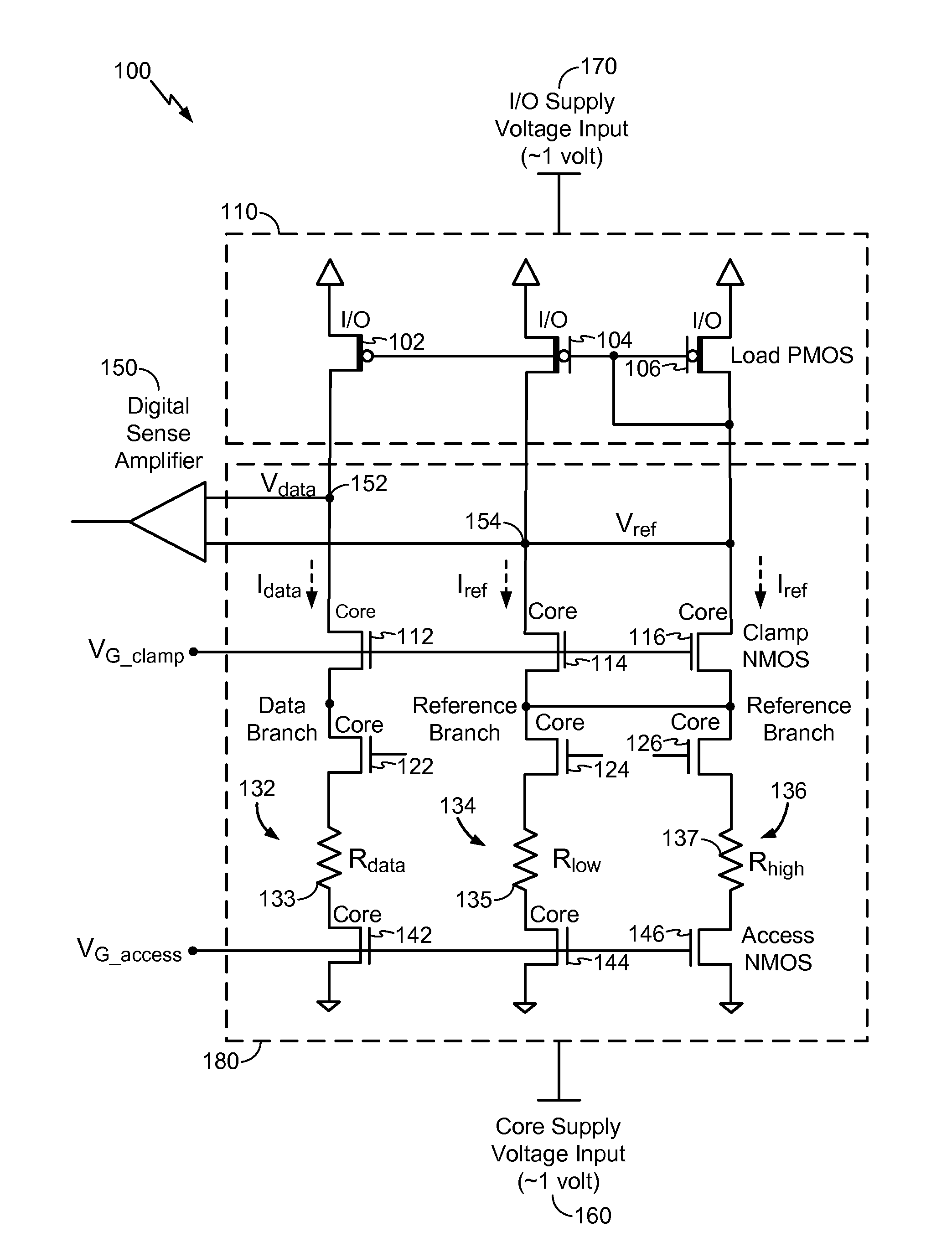
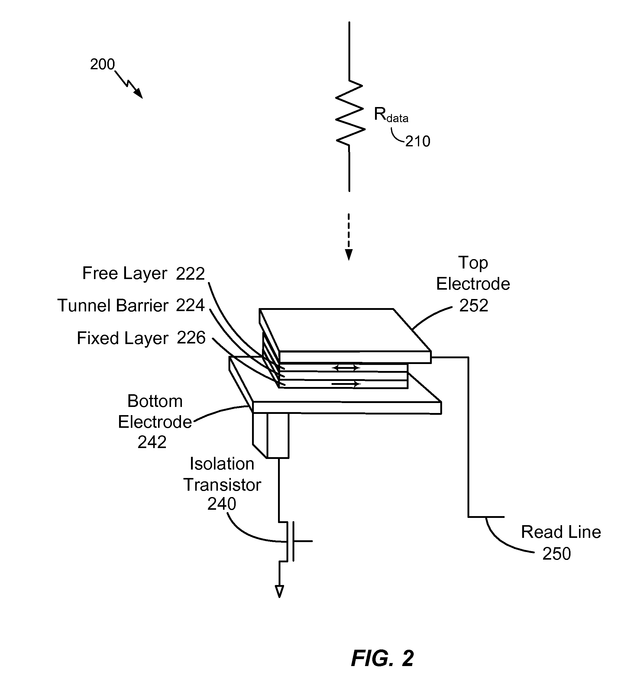
[0028]In a particular illustrative embodiment, input and output (I / O) load transistors are used in a magnetoresistive memory device in place of using core transistors as load transistors to improve the sensing margin of the memory device. I / O load transistors generally have a longer channel length (“length”) than a core transistor. I / O transistors also generally will have a higher supply voltage, a higher threshold voltage, and a higher output resistance than a core transistor, but have a lower current than a core transistor.

[0029]Using core load transistors may result in large variations in sensing margin as a result of process variations in manufacture. A variation in transistors may generally be proportional to the square root of the channel width (“width”) multiplied by the length. For a core transistor, the width multiplied by the length is typically small and, thus, subject to wider proportional variation in manufacture. To provide the same current as a core transistor, an I / O...


PUM


Abstract

A resistance-based memory with a reduced voltage I / O device is disclosed. In a particular embodiment, a circuit includes a data path including a first resistive memory cell and a first load transistor. A reference path includes a second resistive memory cell and a second load transistor. The first load transistor and the second load transistor are input and output (I / O) transistors adapted to operate at a load supply voltage similar to a core supply voltage of a core transistor within the circuit.

Description

FIELD[0001]The present disclosure is generally related to a resistance based memory device.DESCRIPTION OF RELATED ART[0002]It is desirable to continue to increase the density of magnetoresistive random access memory (MRAM) devices such as spin torque transfer MRAM (STT-MRAM) to produce MRAM devices that have increasingly large data storage capacities in increasingly smaller semiconductor devices. Reducing the size of MRAM devices calls for reducing the supply voltage to the MRAM devices. Reducing the supply voltage may reduce MRAM devices' power consumption and heat generation. However, reducing the supply voltage also may reduce the available sensing margin in distinguishing between stored high data values and stored low data values representing logical ones and zeroes, respectively.[0003]Reducing the size of MRAM devices also tends to increase the effect of process variations in the manufacture of such devices. As a result, expected values of operational parameters, such as the se...

Claims


Application Information

Patent Timeline
IPC IPC(8): G11C11/00G11C5/14
CPCG11C11/16G11C11/1673
Inventor JUNG, SEONG-OOKKIM, JISUKANG, SEUNG H.
Owner QUALCOMM INC
Learn More