
Materials for Organic Electroluminescence Devices

a technology of electroluminescence devices and materials, applied in the field of mononuclear, neutral copper (i) complexes, can solve the problems of unachievable colour fidelity, limited number of usable triplet emitters known to date, and difficulty in producing blue-emitting oleds

Inactive Publication Date: 2011-06-30
MERCK PATENT GMBH
View PDF29 Cites 22 Cited by
  • Summary
  • Abstract
  • Description
  • Claims
  • Application Information

AI Technical Summary

Benefits of technology

The patent text describes a new technology for producing opto-electronic components, particularly for display screens and illumination areas. These components are made using mononuclear neutral copper(I) complexes that have a chelating N-heterocyclic ligand and a phosphine or arsine ligand. These complexes have the advantage of being electrically neutral, which makes them more stable and compatible with other components in the device. The patent also discusses the use of triplet emitters, which can be very efficient in producing light in OLEDs. However, there are limitations in the availability of suitable triplet emitters for blue-emitting OLEDs, and the development of blue-emitting OLEDs is still struggling. The patent proposes a solution to these issues by introducing new blue-emitting triplet emitters and discussing their use in OLEDs.

Problems solved by technology

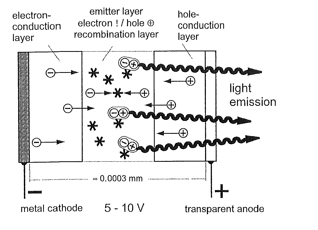
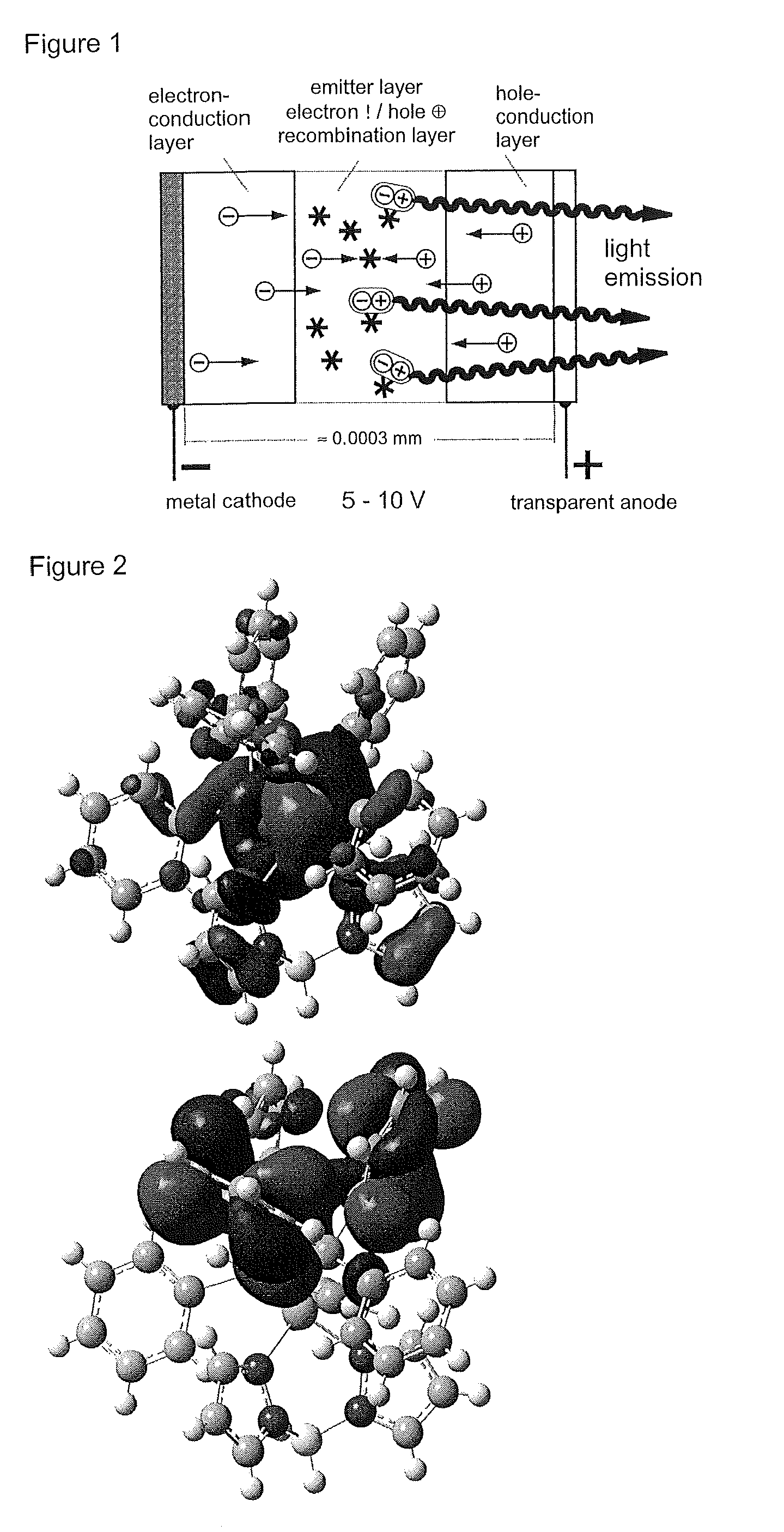
However, it is particularly interesting that it will be possible to produce colour display screens having hitherto unachievable colour fidelity, brightness and viewing-angle independence, having low weight and very low power consumption.
The solutions to date have disadvantages / problems, more precisely in the following areas:long-term stability of the emitters in the OLED devices,thermal stability,chemical stability to water and oxygen,chemical variability,availability of important emission colours,manufacturing reproducibility,achievability of high efficiencies of the conversion of electrical current into light,achievability of very high luminous densities at the same time as high efficiency,use of inexpensive emitter materials,toxicity of the materials used / disposal of used light-emitting elements,development of blue-emitting OLEDs.
However, the production of blue-emitting OLEDs continues to encounter considerable difficulties.
Besides the lack of suitable matrix materials for the emitters, suitable hole- and / or electron-conducting matrix materials, one of the main difficulties is that the number of usable triplet emitters known to date is very limited.
However, the blue-emitting triplet emitters used to date are disadvantageous in a number of respects.
In particular, the synthesis of such compounds requires complex, multistep (for example two or more steps) and time-consuming reactions.
In spite of the great synthetic complexity, only moderate to poor yields are frequently achieved.

Method used


Image

  • Materials for Organic Electroluminescence Devices
  • Materials for Organic Electroluminescence Devices
  • Materials for Organic Electroluminescence Devices

Examples


example 1

[0129]

[0130]Preparation

[0131]A solution of [Cu(CH3CN)4](PF6) (0.186 g, 0.500 mmol) and bis(2-diphenyl-phosphinophenyl)ether (pop, 0.269 g, 0.500 mmol) in acetonitrile (15 ml) is stirred for 30 min. under an argon atmosphere. K[H2Bpz2] (0.093 g, 0.500 mmol) is then added to the solution, and the resultant mixture is stirred for a further 2 hours under an argon atmosphere. The resultant white precipitate is filtered off and washed three times with 5 ml of acetonitrile. Yield 0.313 g, 84%.

[0132]1H-NMR (CDCl3, 298 K): δ 7.59 (d, 2H), 7.05-7.22 (m, br, 20H), 6.78-6.87 (m, br, 6H), 6.68-6.71 (m, br, 2H), 5.84 (t, 2H), 5.30 (s, 2H). 13C{1H}-NMR: δ 128.2, 129.2, 130.6, 132.8, 134.0, 134.3, 140.1. 31P{1H}-NMR: δ−17.23 (s), −18.75 (s). ES-MS: m / e=749.3 (MH+, 100.0%), 750.3 (58.0%), 748.2 (24.0%), 752.3 (21.5%), 753.3 (4.8%). EA: found C, 61.72; H, 4.52; N, 6.72%; calc. C, 61.93; H, 4.59; N, 6.72 (for C43H38BCuN4OP2Cl2).

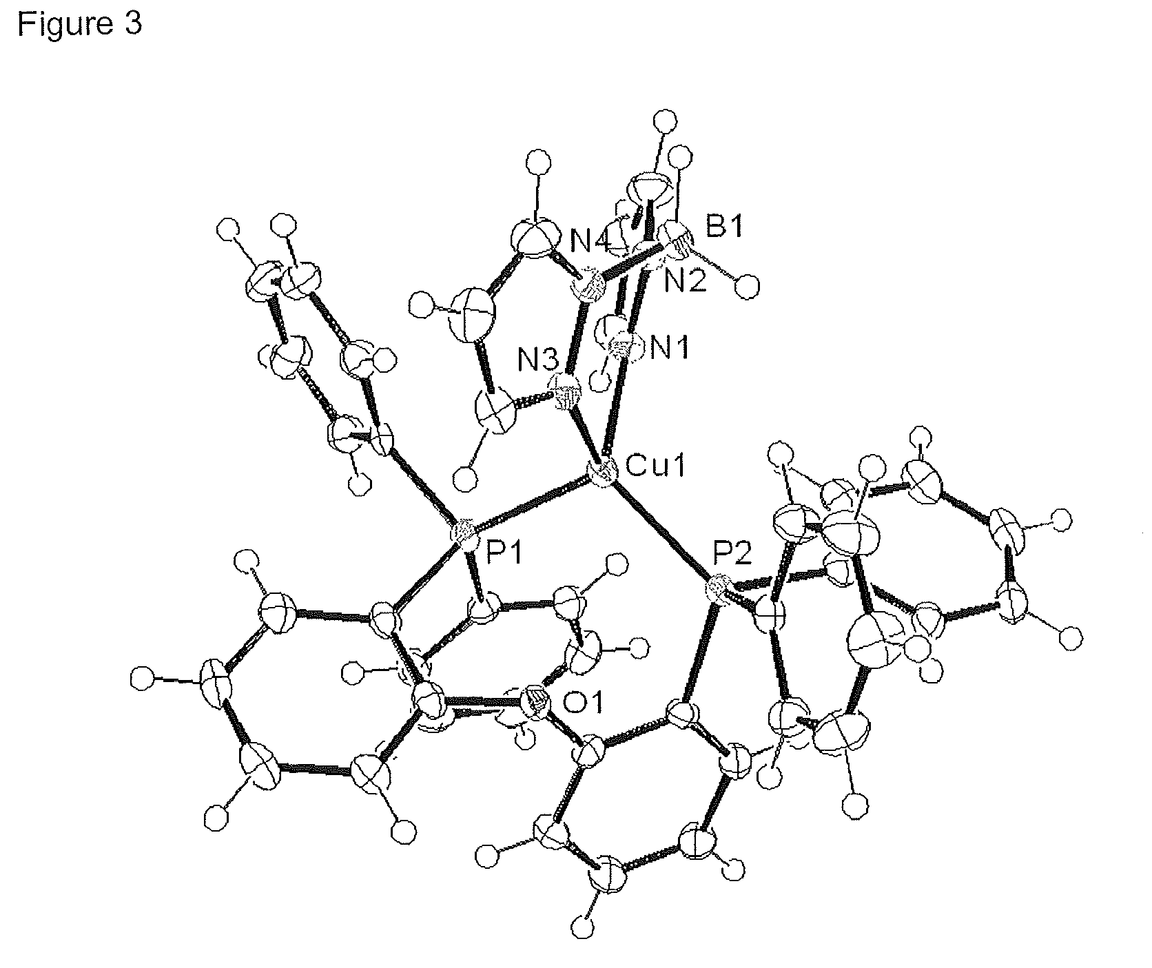
[0133]Crystal Structure

[0134]An ORTEP image of this complex is shown in FI...

example 2

[0137]

[0138]Preparation

[0139]The synthetic route is analogous to [Cu(H2Bpz2)(pop)] (Example 1). Yield 81%.1H-NMR (CDCl3, 298 K): δ 7.52 (d, 2H), 7.35-7.29 (m, br, 10H), 7.22 (d, 4H), 7.12 (t, 8H), 6.99 (td, 2H), 6.86 (td, 2H), 6.72-6.67 (m, br, 2H), 6.61-6.58 (m, 2H), 5.76 (d, 2H), 1.46 (s, 6H). 13C{1H}-NMR: δ 14.07, 103.1, 119.6, 124.1, 128.1, 128.2, 129.2, 130.4, 132.5, 132.6, 133.8, 133.4, 134.5, 134.7, 135.4, 148.9, 157.0. 31P{1H}-NMR: δ 14.89 (s), −16.18 (s), −17.14 (s). ES-MS: m / e=MH+, 772.2 (100.0%), 778.2 (57.0%), 780.2 (22.2%), 781.2 (6.8%). EA: found C, 68.45; H, 5.10; N, 7.33%; calc. C, 68.00; H, 5.19; N, 7.21 (for C49H43BCuN8OP2Cl2).

[0140]Crystal Structure

[0141]An ORTEP image of this complex is shown in FIG. 5.

[0142]Photoluminescence Properties

[0143]The photoluminescence properties of this complex are shown in FIG. 6.

example 3

[0144]

[0145]Preparation

[0146]The synthetic route is analogous to [Cu(H2Bpz2)(pop)] (Example 1). Yield 79%. 1H-NMR (CDCl3, 298 K): δ 7.38 (br, 4H), 7.05-7.24 (m, br, 20H), 6.76-6.98 (m, br, 6H), 6.68-6.71 (m, br, 2H), 5.85 (t, 4H), 5.30 (s, 4H). 13C{1H}-NMR: δ 104.4, 106.3, 120.3, 124.4, 124.8, 126.4, 128.2, 128.3, 128.5, 128.6, 129.3, 129.7, 130.8, 131.5, 131.6, 131.8, 132.0, 133.2, 133.3, 133.4, 133.8, 134.0, 134.1, 135.3, 135.9, 141.7, 157.8, 157.9, 158.1. 31P{1H}-NMR: δ−14.37 (s). ES-MS: m / e=881.4 (MH+, 100.0%), 882.4 (63.0%), 883.4 (59.0%), 884.3 (26.1%), 880.4 (23.2%), 885.4 (6.3%), 886.3 (1.4%). EA: found C, 61.55; H, 4.48; N, 11.63%; calc. C, 60.85; H, 4.48; N, 11.59 (for C49H43BCuN8OP2Cl2).

[0147]Crystal Structure

[0148]An ORTEP image of this complex is shown in FIG. 7.

[0149]Photoluminescence Properties

[0150]The photoluminescence spectrum of this complex is shown in FIG. 5.


PUM

PropertyMeasurementUnit
thicknessaaaaaaaaaa
voltageaaaaaaaaaa
pressureaaaaaaaaaa

Abstract

The invention relates to mononuclear, neutral copper (1) complexes having a bidentate ligand that binds via nitrogen, and two phosphane or arsane ligands, to the use thereof for producing electronic components, and to electronic devices comprising said complexes.

Description

[0001]The invention relates to mononuclear neutral copper(I) complexes of the formula A ([(N∩N)CuL2]) and to the use thereof for the production of opto-electronic components,where N∩N stands for a chelating N-heterocyclic ligand, which is bonded to the copper atom via two nitrogen atoms, and L is, independently of one another, a phosphine or arsine ligand. The two ligands L may also be bonded to one another, giving rise to a divalent ligand. In this case, either a) N∩N must be mononegative and the two ligands (phosphine or arsine ligands) must be neutral (preferred embodiment) or b) N∩N must be neutral and the two phosphine / arsine ligands taken together must be mono-negatively charged, so that the mononuclear copper(I) complex is electrically neutral.INTRODUCTION [0002]A change is currently evident in the area of display screen and illumination technology. It will be possible to manufacture flat displays or lighting areas with a thickness of less than 0.5 mm. These are distinguished...

Claims


Application Information

Patent Timeline
Patent Type & Authority Applications(United States)
IPC IPC(8): C09K11/06C07F5/02B05D5/06H10K99/00
CPCH01L51/0037H01L51/008H01L51/0091H01L51/0094H01L51/5012H01L2251/5384Y10S428/917C09B57/10C09K2211/188C09K11/06C09K2211/1044C09K2211/1085C07F5/02Y02E10/549C07F9/5045H10K85/1135H10K85/322H10K85/371H10K85/40H10K50/11H10K2101/90C07F1/08H10K85/00H10K85/111
Inventor YERSIN, HARTMUTUWE, MONKOWIUSCZERWIENIEC, RAFALYU, JIANGBO
Owner MERCK PATENT GMBH
Learn More