
Method of programming an electrically programmable and erasable non-volatile memory point, and corresponding memory device

a non-volatile memory, electrically erasable technology, applied in the field of memory, can solve the problems of reducing the chances affecting the production process of the memory plane, and affecting the effect of the control design, so as to reduce the chance of a short circuit

Active Publication Date: 2011-06-16
STMICROELECTRONICS (ROUSSET) SAS
View PDF4 Cites 3 Cited by
  • Summary
  • Abstract
  • Description
  • Claims
  • Application Information

AI Technical Summary

Benefits of technology

[0005]This approach reduces the constraint on the voltage capacity of the transistors. However, it may have the drawback of making the memory plane production process more complicated, as a “triple case” technology is used because of the negative voltage of several volts. Furthermore, the control design may be relatively more complicated because negative switching voltages are provided, which also may have a negative effect on the area of the memory plane. This may be because negative voltage switching may be relatively costly in terms of memory plane area (use of p-type metal oxide semiconductor (PMOS) transistors) where the control gate selection transistors are concerned, and may be inappropriate for the low granularity of EEPROMs.
[0006]In one form of application and embodiment, a method for programming an electrically programmable and erasable non-volatile memory point, with a corresponding memory device, which is compatible with a conventional approach for producing memories of this type is described. In other words, it may involve relatively little, for example, modification of the production process, and may be compatible with byte granularity. The method may reduce the production constraints on the voltage capacity of the transistors and considerably increase the reliability by reducing the risk of oxide breakdown.
[0008]This is because a relatively small variation in the programming voltage may be sufficient to have a considerable (exponential) effect on the reliability of the memory points with respect to gate oxide breakdown. Additionally, by using a negative voltage below the threshold value of a PN diode, for example a negative voltage of about 500 millivolts, it may be possible to achieve this considerable effect on the reliability of the memory points while retaining the compatibility with a conventional EEPROM memory point production process, using a “single well” technology, for example. This low negative voltage may be compatible with such a technology, because it may avoid the avalanching of the PN junctions.
[0009]Additionally, the memory point may short-circuit the bit line and the ground line in the erase phase. The simultaneous application of the negative voltage to the bit line and the ground line (instead of the conventional application of the ground voltage (in other words, 0 volts on the ground line)) may reduce the chances of a short circuit between the negative voltage and 0 volts.

Problems solved by technology

However, it may have the drawback of making the memory plane production process more complicated, as a “triple case” technology is used because of the negative voltage of several volts.
Furthermore, the control design may be relatively more complicated because negative switching voltages are provided, which also may have a negative effect on the area of the memory plane.
This may be because negative voltage switching may be relatively costly in terms of memory plane area (use of p-type metal oxide semiconductor (PMOS) transistors) where the control gate selection transistors are concerned, and may be inappropriate for the low granularity of EEPROMs.

Method used


Image

  • Method of programming an electrically programmable and erasable non-volatile memory point, and corresponding memory device
  • Method of programming an electrically programmable and erasable non-volatile memory point, and corresponding memory device
  • Method of programming an electrically programmable and erasable non-volatile memory point, and corresponding memory device

Examples


Embodiment Construction

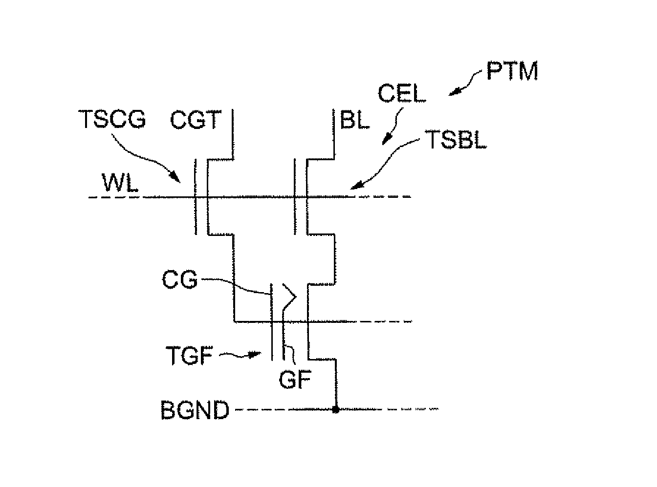
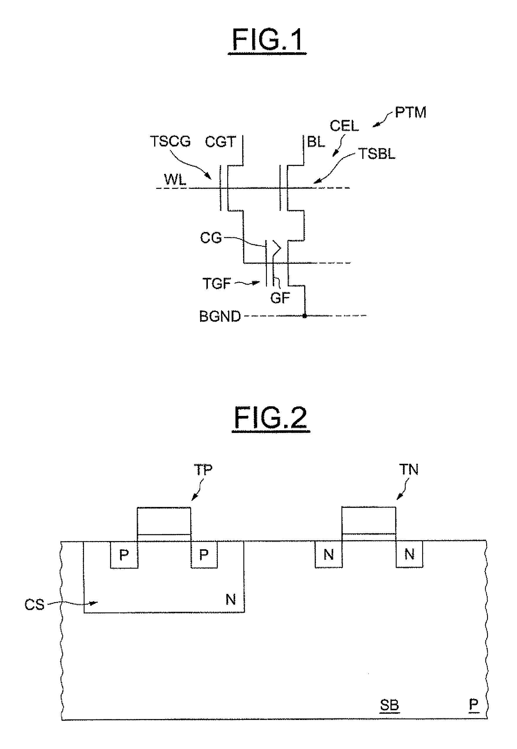
[0034]An example of the architecture of memory points is illustrated in FIG. 1. In this drawing, the memory point PTM has a memory cell CEL including a transistor TGF having a control gate CG and a floating gate GF. The cell CEL is connected to a bit line BL through a bit line selection transistor TSBL.

[0035]The cell also includes a control gate selection transistor TSCG connected between a gate control line CGT and the control gate CG of the floating-gate transistor TGF. The gates of the transistors TSCG and TSBL are connected to a word line WL extending in a conventional way perpendicularly to the bit line BL. The source of the transistor TGF is connected to a ground line BGND.

[0036]The architecture of FIG. 1 therefore provides one cell memory for each bit. This memory point can be programmed, that is, written to or erased, or read.

[0037]Generally, words of x bits, typically eight bits, forming bytes, are stored in an EEPROM. Typically, therefore, the storage area for a byte has e...


PUM


Abstract

An electrically programmable and erasable non-volatile memory point may have at least one floating-gate transistor connected to a bit line and to a ground line, and may be programmed with a programming voltage. In an erase phase of the memory point, a first, negative, voltage may be applied to the bit line and to the ground line. The absolute value of the first voltage may be smaller than a threshold value of a PN diode. A second positive voltage which is smaller than the programming voltage may be applied to the control gate of the floating-gate transistor. The difference between the second voltage and the first voltage may be equal to the programming voltage, and, in a writing phase, the first negative voltage may be applied to the control gate of the floating-gate transistor, and the second voltage may be applied to the bit line.

Description

FIELD OF THE INVENTION[0001]The invention relates to memories, more specifically electrically erasable and programmable non-volatile memories (EEPROMs).BACKGROUND OF THE INVENTION[0002]In an EEPROM, the logical value of a bit stored in a memory point may be represented by a threshold voltage of a floating-gate transistor, which may be modified by writing or erase operations. Writing or erasing may be carried out on a floating-gate transistor by injecting electrical charges into the transistor gate, or removing them from it, by a tunnel effect (the Fowler-Nordheim effect), using a high programming voltage Vpp which may be about 10 to 20 volts, and is typically 16 volts.[0003]This high voltage of 16 volts, which is generally required for programming EEPROMs, may not be reduced and may set considerable constraints on the processing and reliability of the product. This is because the lithographic reduction, i.e. the increase of the etching resolution, tends to decrease the operating vol...

Claims


Application Information

Patent Timeline
Patent Type & Authority Applications(United States)
IPC IPC(8): G11C16/04G11C16/12G11C16/14
CPCG11C16/30G11C16/10
Inventor TAILLIET, FRANCOIS
Owner STMICROELECTRONICS (ROUSSET) SAS
Learn More