Semiconductor device

a technology of semiconductors and semiconductors, applied in the direction of solid-state devices, climate sustainability, instruments, etc., can solve the problems of increasing the cost per storage capacity, difficult to sufficiently reduce power consumption, short data holding time, etc., and achieves the effects of reducing power consumption, ensuring data is retained for an extremely long time, and reducing the frequency of refresh operation

Active Publication Date: 2011-05-05
SEMICON ENERGY LAB CO LTD
View PDF78 Cites 512 Cited by
  • Summary
  • Abstract
  • Description
  • Claims
  • Application Information

AI Technical Summary

Benefits of technology

[0025]Since the off current of a transistor including an oxide semiconductor is extremely low, stored data can be retained for an extremely long time by using the transistor. In other words, power consumption can be considerably reduced because refresh operation becomes unnecessary or the frequency of refresh operation can be extremely low. Moreover, stored data can be retained for a long time even when power is not supplied.
[0026]Further, high voltage is not needed to write data, and deterioration of the element is negligible. Furt

Problems solved by technology

Moreover, a transistor included in a memory element has a leakage current and charge flows into or out of a capacitor even when the transistor is not selected, so that the data holding time is short.
For that reason, another writing operation (refresh operation) is necessary at predetermined intervals, and it is difficult to sufficiently reduce power consumption.
Furthermore, since stored data is lost when power supply stops, an additional memory device using a magnetic material or an optical material is needed in order to hold the data for a long time.
However, cost per storage capacity is increased because a circuit such as a flip-flop is used.
Moreover, as in a DRAM, s

Method used


Image

  • Semiconductor device
  • Semiconductor device
  • Semiconductor device

Examples


embodiment 1

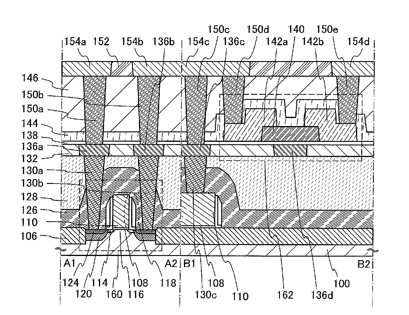
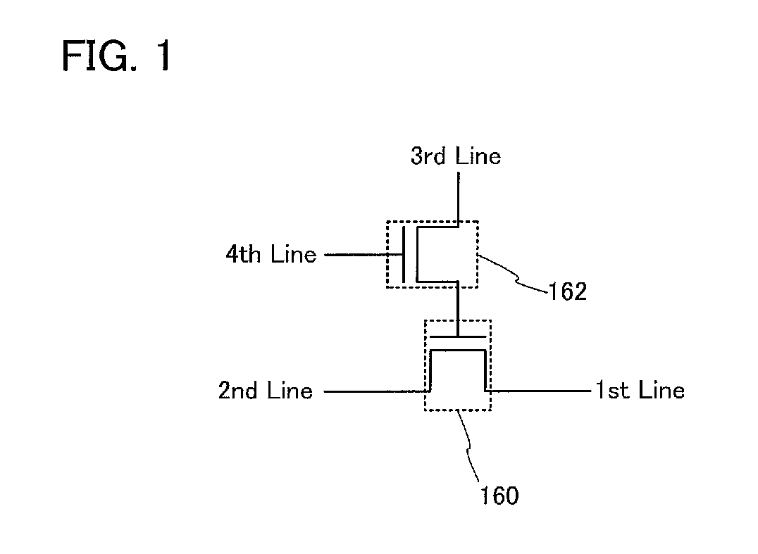
[0064]In this embodiment, a structure and a manufacturing method of a semiconductor device according to one embodiment of the invention disclosed herein will be described with reference to FIG. 1, FIGS. 2A and 2B, FIGS. 3A to 3H, FIGS. 4A to 4GFIGS. 5A to 5D, FIG. 6, FIGS. 7A and 7B, FIGS. 8A and 8B, and FIGS. 9A and 9B.

[0065]FIG. 1 illustrates an example of a circuit configuration of a semiconductor device. The semiconductor device includes a transistor 160 formed using a material other than an oxide semiconductor (e.g., silicon), and a transistor 162 formed using an oxide semiconductor. Note that the semiconductor device illustrated in FIG. 1 is called a memory cell in some cases in the following description.

[0066]Here, a gate electrode of the transistor 160 is electrically connected to one of a source electrode and a drain electrode of the transistor 162. A first line (also referred to as a source line SL) is electrically connected to a source electrode of the transistor 160. A s...

modification example

[0188]FIG. 6, FIGS. 7A and 7B, FIGS. 8A and 8B, and FIGS. 9A and 9B illustrate modification examples of structures of semiconductor devices. The semiconductor devices in each of which the transistor 162 has a structure different from that described above will be described below as modification examples. That is, the structure of the transistor 160 is the same as the above.

[0189]FIG. 6 illustrates an example of a semiconductor device including the transistor 162 in which the gate electrode 136d is placed below the oxide semiconductor layer 140 and the source / drain electrodes 142a and 142b are in contact with a bottom surface of the oxide semiconductor layer 140. Note that the planar structure can be changed as appropriate to correspond to the cross section; therefore, only the cross section is shown here.

[0190]A large difference between the structure in FIG. 6 and the structure in FIG. 2A is the position at which the oxide semiconductor layer 140 is connected to the source / drain elec...

embodiment 2

[0216]In this embodiment, a structure and a manufacturing method of a semiconductor device, according to another embodiment of the disclosed invention, will be described with reference to FIGS. 15A and 15B.

[0217]FIG. 15A illustrates an example of a circuit configuration of a semiconductor device. FIG. 15A is different from FIG. 1 in that a capacitor 164 is provided. That is, in FIG. 15A, one of a source electrode and a drain electrode of the transistor 162, one of electrodes of the capacitor 164, and a gate electrode of the transistor 160 are electrically connected to one another. A first line (also referred to as a source line BL) and a source electrode of the transistor 160 are electrically connected to each other, and a second line (also referred to as a bit line BL) and a drain electrode of the transistor 160 are electrically connected to each other. A third line (also referred to as a first signal line S1) and the other of the source electrode and the drain electrode of the tra...


PUM


Abstract

Disclosed is a semiconductor device capable of functioning as a memory device. The memory device comprises a plurality of memory cells, and each of the memory cells contains a first transistor and a second transistor. The first transistor is provided over a substrate containing a semiconductor material and has a channel formation region in the substrate. The second transistor has an oxide semiconductor layer. The gate electrode of the first transistor and one of the source and drain electrodes of the second transistor are electrically connected to each other. The extremely low off current of the second transistor allows the data stored in the memory cell to be retained for a significantly long time even in the absence of supply of electric power.

Description

TECHNICAL FIELD[0001]The invention disclosed herein relates to a semiconductor device using a semiconductor element and a method for manufacturing the semiconductor device.BACKGROUND ART[0002]Memory devices using semiconductor elements are broadly classified into two categories: a volatile device that loses stored data when power supply stops, and a non-volatile device that retains stored data even when power is not supplied.[0003]A typical example of a volatile memory device is a DRAM (dynamic random access memory). A DRAM stores data in such a manner that a transistor included in a memory element is selected and charge is stored in a capacitor.[0004]When data is read from a DRAM, charge in a capacitor is lost on the above-described principle; thus, another writing operation is necessary whenever data is read out. Moreover, a transistor included in a memory element has a leakage current and charge flows into or out of a capacitor even when the transistor is not selected, so that th...

Claims


Application Information

Patent Timeline
IPC IPC(8): H01L27/13
CPCG11C11/405G11C16/0433H01L21/8258H01L27/0207H01L27/105H01L27/11519H01L29/7833H01L27/11524H01L27/11551H01L27/1156H01L27/1225H01L28/60H01L27/11521H10B41/10H10B41/70H10B41/20H10B41/30H10B41/35Y02D10/00H01L29/06H01L29/78693H01L21/02664H01L21/46H01L29/7869
Inventor YAMAZAKI, SHUNPEI
Owner SEMICON ENERGY LAB CO LTD
Why Eureka
Try Eureka