
Chip integrated ion sensor

a technology of integrated ion sensors and ion sensors, which is applied in the direction of instruments, semiconductor devices, measurement devices, etc., can solve the problems of hardly being miniaturised and integrated into silicon chips, hardly being integrated into cmos chips, and conventional isfets are very small, and achieve the effect of easy manufacturing

Inactive Publication Date: 2011-05-05
NXP BV
View PDF10 Cites 13 Cited by
  • Summary
  • Abstract
  • Description
  • Claims
  • Application Information

AI Technical Summary

Benefits of technology

The present invention provides an alternative ion sensor that is easy to manufacture and can be integrated into a chip. The ion sensor includes a substrate with an electrolyte insulator semiconductor structure and a reference electrode. The substrate can be processed using standard semiconductor processes and the method of manufacturing the ion sensor can be easily integrated into existing chip manufacturing processes. The ion sensor can be used as a pH sensor or in other applications where the detection of ions is necessary. The method of manufacturing the ion sensor is simple and can be used in a wide range of applications. The ion sensor is protected from degrading and the thickness of the dielectric layer can be adjusted to achieve desired sensitivity. The sensor electrode can form a second electrode of the capacity or a sensing capacity. The semiconductor material can be doped and the amount of dopant can be predetermined to achieve a desired level of sensitivity.

Problems solved by technology

Because of size and / or detection principle they can hardly be miniaturised and integrated into a silicon chip.
Conventional ISFETs are very small but cannot be integrated into a CMOS chip because the direct contact of the liquid with the gate dielectric can also affect other transistors in close proximity and destroy the device due to corrosion and uptake of ions (shift in threshold voltage of transistors caused by Na diffusing into the gate regions).

Method used


Image

  • Chip integrated ion sensor
  • Chip integrated ion sensor
  • Chip integrated ion sensor

Examples


Embodiment Construction

[0042]The illustration in the drawing is schematically. In different drawings, similar or identical elements are provided with similar or identical reference signs.

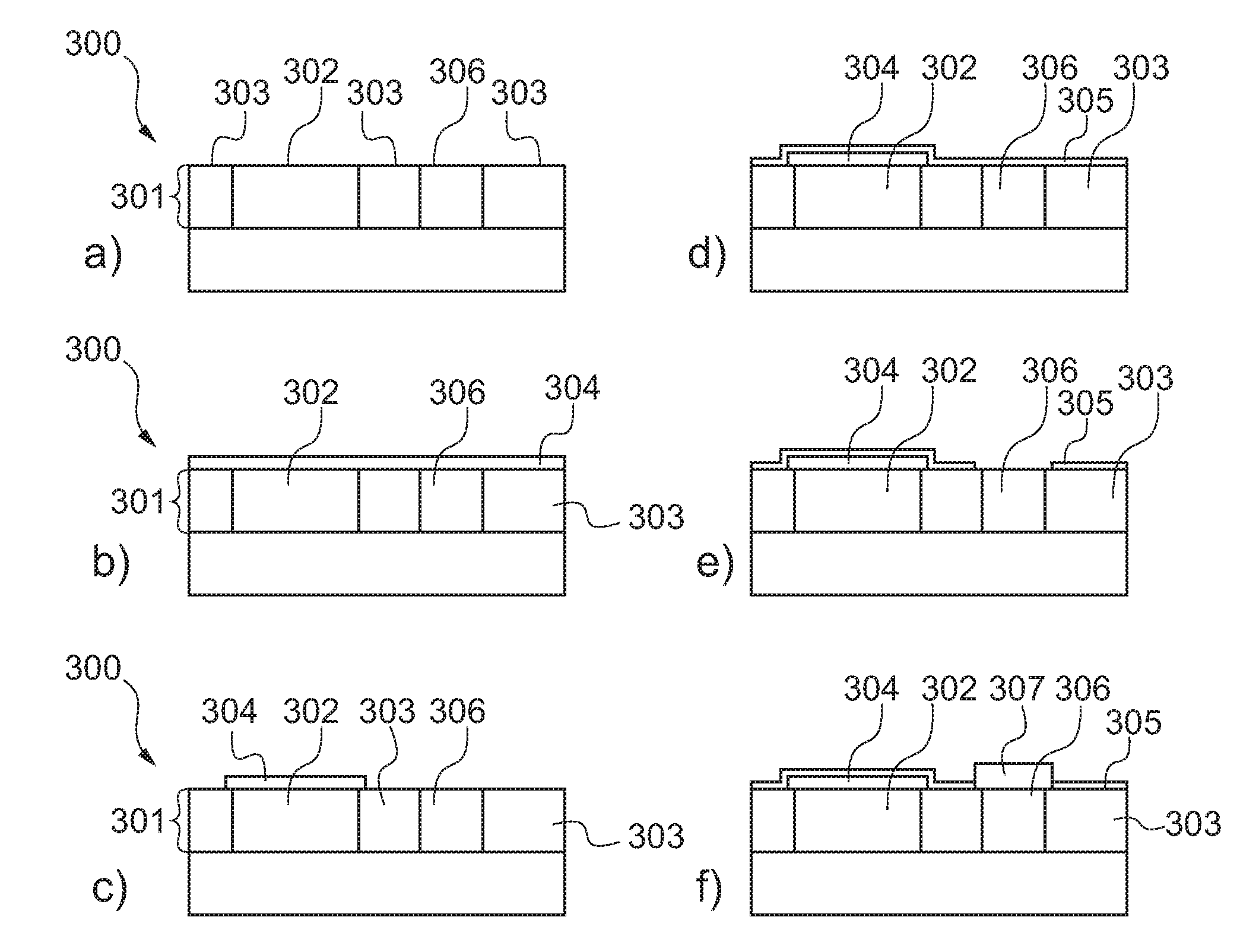
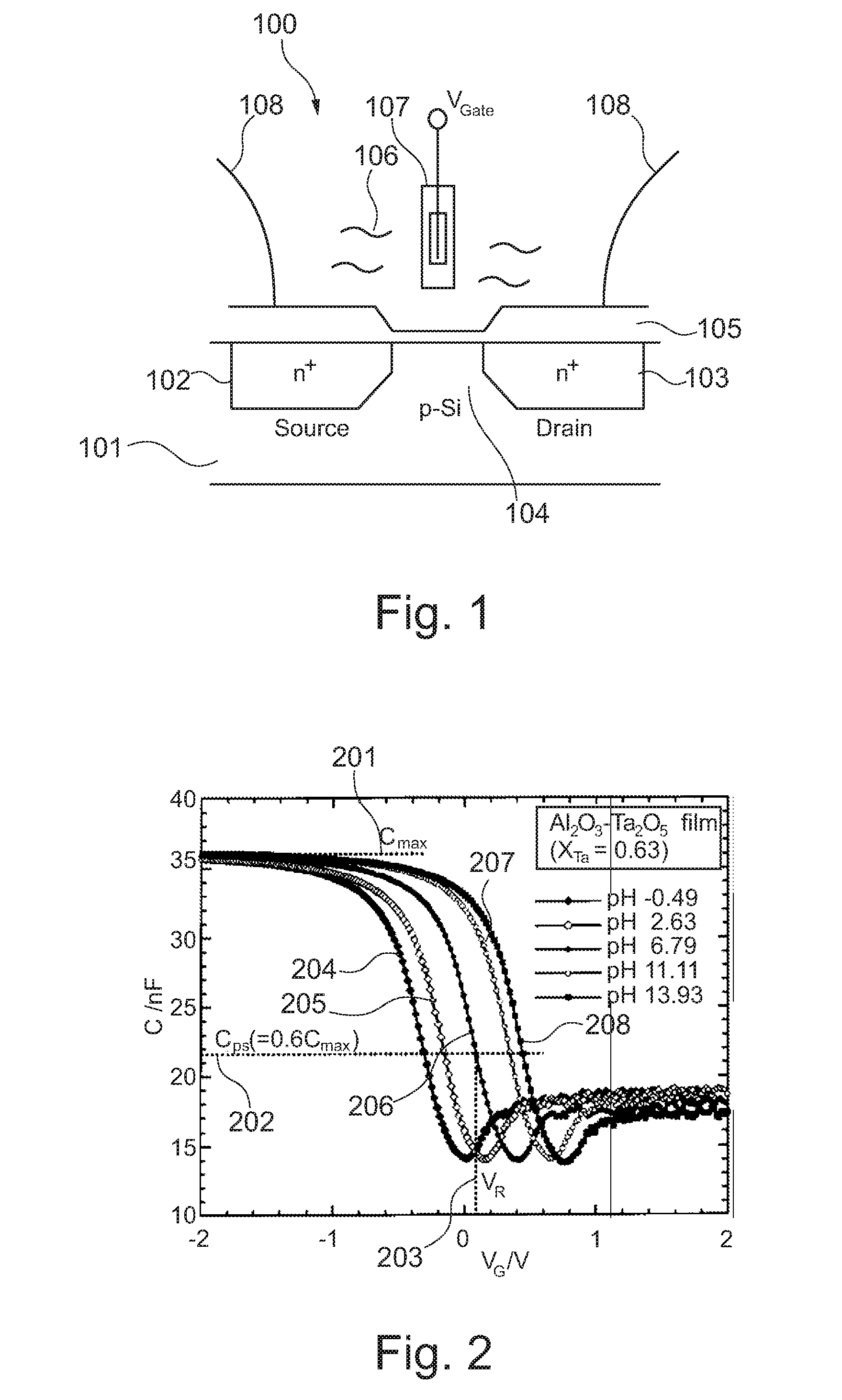
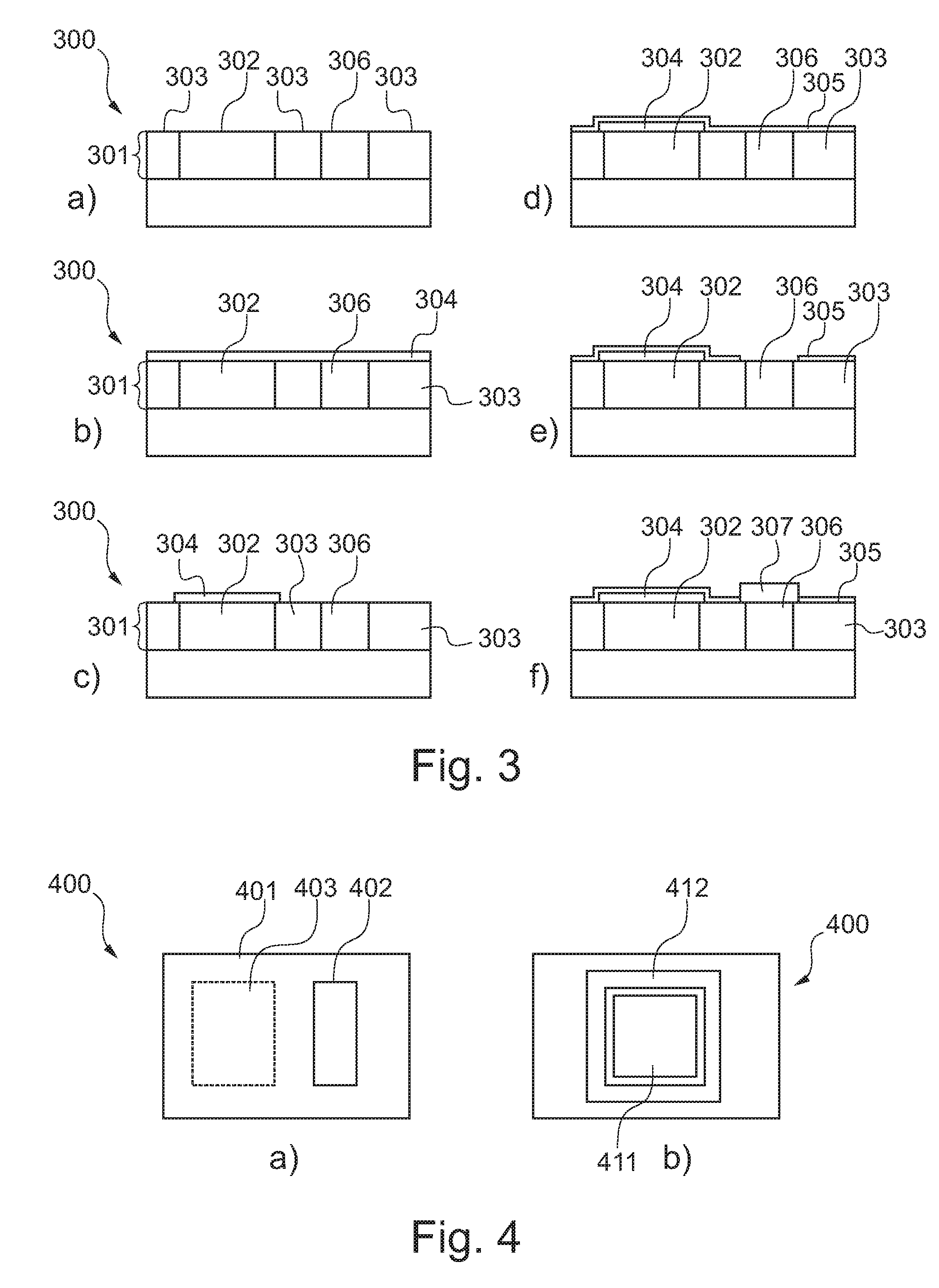
[0043]In the following an exemplary embodiment of a chip integrated ion sensor will described in more detail with reference to the FIGS. 1 to 4.

[0044]FIG. 1 schematically illustrates an Ion Sensitive Field Effect Transistor (ISFET) 100 which is helpful for understanding the present invention and which is described in “Thirty years of ISFETOLOGY What happened in the past 30 years and what may happen in the next 30 years. P. Bergveld, Sensors and Actuators B 88 (2003) 1-20. The ISFET 100 comprises a substrate 101 in which a source region 102 and a drain region 103 is formed. Between the source and the drain regions a channel region 104 is formed and a gate insulating layer 105 is formed on top of the source region 102, drain region 103 and channel region 104. An electrolyte 106 to be analyzed may be brought into contact wit...


PUM

PropertyMeasurementUnit
thicknessaaaaaaaaaa
thicknessaaaaaaaaaa
thicknessaaaaaaaaaa

Abstract

A chip integrated ion sensor is provided, which comprises a substrate having arranged thereon an electrolyte insulator semiconductor structure and a reference electrode. In particular, the electrolyte insulator semiconductor (EIS) structure may be formed on a chip already processed, i.e. the EIS structure may be formed in a Back End process on an already formed chip comprising a plurality of formed electronic components. In particular, the ion sensor may be adapted to form an ion concentration sensor, e.g. a pH sensor, i.e. may form a pH sensor. The reference electrode may be a non-polarizable electrode. In particular, the reference electrode may comprise Ag or AgCl as material.

Description

FIELD OF THE INVENTION[0001]The invention relates to a chip integrated ion sensor, in particular to a chip integrated ion concentration sensor for producing a signal indicative of an ion concentration within a solution.[0002]The invention further relates to a method of producing a chip integrated ion sensor.BACKGROUND OF THE INVENTION[0003]Nowadays a plurality of sensors is integrated into electronic chips. For example, it is interesting to implement pH sensors into electronic chips, since the pH value is an integral parameter of every (aqueous) solution, it describes to which degree the solution is alkaline or acidic. Over a wide range it is well approximated by: pH=−log [H+] with [H+] denoting the proton concentration of the solution in mol / L. pH measurement is a routine task in industry and laboratories for process control and analysis. However, it could also become interesting for a wider application range if the cost of the pH measurement units (sensor plus electronics) become ...

Claims


Application Information

Patent Timeline
Patent Type & Authority Applications(United States)
IPC IPC(8): G01N27/414H01L29/772H01L21/335
CPCG01N27/227
Inventor MERZ, MATTHIAS
Owner NXP BV
Learn More