
Fault diagnosis in a memory bist environment

a memory bist environment and fault diagnosis technology, applied in the field of memory bist environment fault diagnosis, can solve the problems of many types of failures, time-related or complex read faults, and the difficulty of testing and diagnosing embedded memory systems, so as to reduce the time to transfer diagnostic data, speed up the extraction of diagnostic data, and recover failure data. the effect of safety

Inactive Publication Date: 2011-03-03
MENTOR GRAPHICS CORP
View PDF12 Cites 29 Cited by
  • Summary
  • Abstract
  • Description
  • Claims
  • Application Information

AI Technical Summary

Benefits of technology

[0014]Various aspects of the invention relate to techniques and devices for temporally compacting test response signatures of failed memory tests in a memory built-in self-test environment, to provide the ability to carry on memory built-in self-test operations even with the detection of multiple time related memory test failures. In some implementations of the invention, the compacted test response signatures are provided to an ATE along with memory location information. A diagnostic tool may receive the compacted test response signatures and memory location information from the ATE. Then, using the memory location information, the diagnostic tool may select an appropriate diagnostic procedure for a compacted test response signature to provide very time-efficient off-line routines to safely recover failure data from the compacted test response signatures.
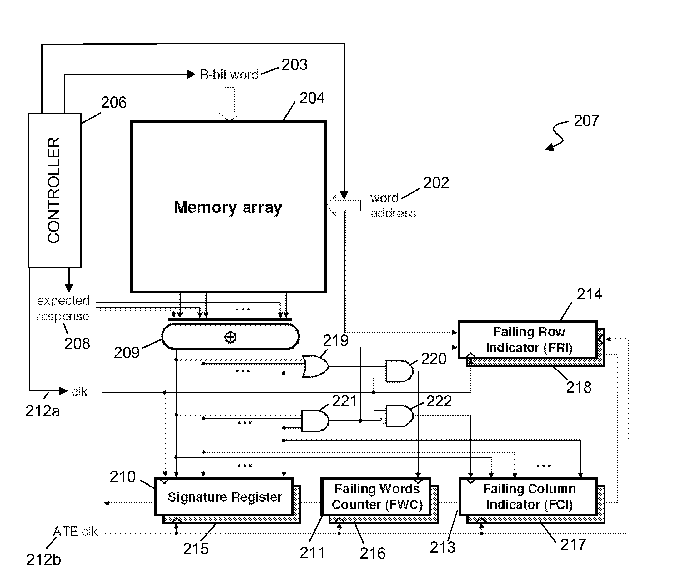
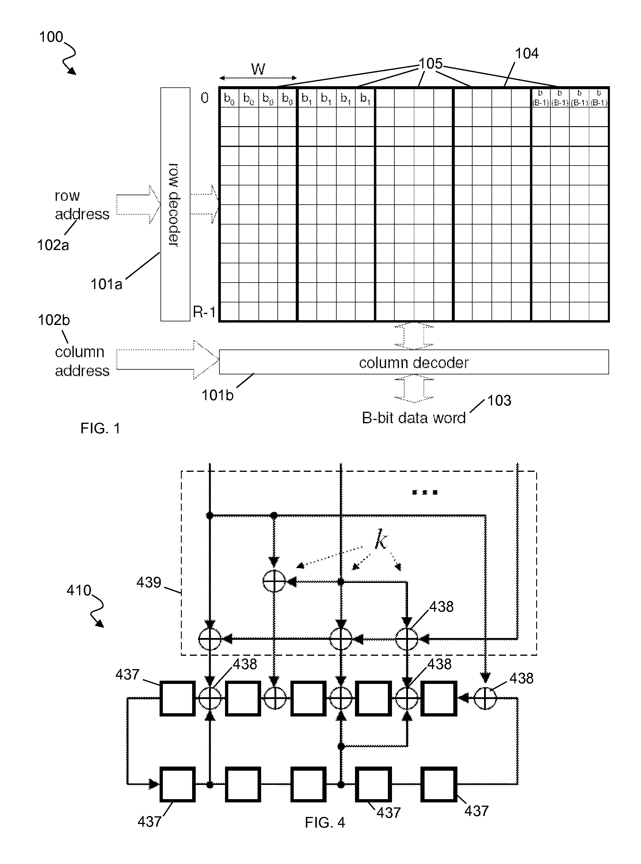
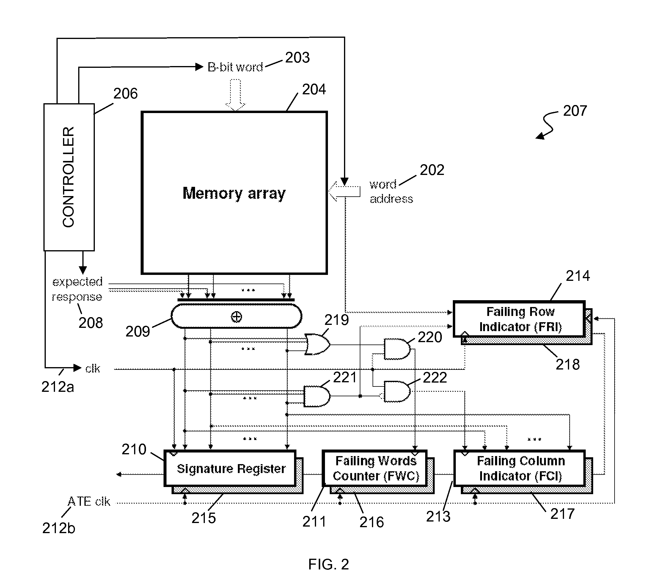
[0015]According to various implementations of the invention, an integrated circuit with embedded memory and a memory BIST controller also includes a linear feedback structure for use as a signature register that can temporally compact test response signatures from the embedded memory array during a test step of a memory test. The linear feedback structure may be, for example, a linear feedback shift register. In various implementations, the integrated circuit may also include a failing words counter, a failing column indicator, and / or a failing row indicator. The failing words counter, failing column indicator, and failing row indicator collect memory location information whenever the linear feedback structure compacts a failing test response. With these implementations, on-chip compression of diagnostic data, that is, test response data and location data, reduces the time to transfer the diagnostic data to the ATE.
[0016]According to various other implementations of the invention, a diagnostic tool receives the diagnostic data from the ATE, and selects an appropriate diagnostic technique by using a lookup table. The values stored by the failing words counter, the failing column indicator, and the failing row indicator may serve as indices for the look-up table. Moreover, the diagnostic tool may employ additional look-up tables to speed up extraction of diagnostic data from the compressed test responses. In this way, time to test and amount of test data provided to the ATE and received by the diagnostic tool from the ATE can be significantly reduced. These and other features and aspects of the invention will be apparent upon consideration of the following detailed description.

Problems solved by technology

Due to their extremely large scale of integration, memory arrays have already started introducing new yield loss mechanisms at a rate, magnitude, and complexity large enough to demand major changes in test strategies.
Indeed, many types of failures, such as time-related or complex read faults, often not seen earlier, originate in the highest density areas of semiconductor chips.
In contrast to stand-alone memory units, however, embedded memory systems are more difficult to test and diagnose.
This difficulty arises not only because of the more complex structure of embedded memories, but also because of the decreasing number of inputs and outputs available to access and control these circuits, resulting in a reduced bandwidth of test channels.
However, relatively low bandwidth at the I / O channels of the integrated circuit device can make it difficult or impossible to quickly download failing signatures or address locations of failing sites of the embedded memory.
This problem grows in significance when another fault is detected while downloading previously obtained diagnostic data.
When this is the case, the BIST controller can continue to test while encountering failures, until the registers are filled.
It is worth noting that certain single faults may produce large amounts of diagnostic data.
For example, a failure in just one signal line or “interconnect” could result in an entire row or column of the memory array working incorrectly, producing a great deal of erroneous data.
First of all, it may take a significant amount of time to scan the data out.
Second, the ATE memory may get filled up very quickly, especially if all memory failures are being recorded.
Truncation of data is typically not acceptable from a diagnostic point of view.
Also, a lengthy unloading of the ATE memory is often unacceptable due to time constraints.

Method used


Image

  • Fault diagnosis in a memory bist environment
  • Fault diagnosis in a memory bist environment
  • Fault diagnosis in a memory bist environment

Examples


example 1

[0116]Assume a single faulty cell cx produces the signature S(cx) 1654 in FIG. 16. FIG. 16 shows a signature register trajectory in a multiple input ring generator. In various embodiments, the reference distance Lref 1655 between the initial state (0 . . . 0001) and the state corresponding to the faulty rightmost cell c0 in the last row (R-1) is determined from its signature S(c0) 1656. This state can be obtained as a result of a single injection to the empty MIRG at input b1 (see FIG. 13). Next, the distance Lx 1657 between the initial state (0 . . . 0001) and the actual state of the MIRG is determined. The location of the faulty cell cx is x=Lx−Lref. 1658.

example 2

[0117]Consider a single column failure producing signature S(Cx). FIG. 17 illustrates a single column failure Cx and the reference column C. Here, the rightmost column C0 of a given vertical segment of the memory array assumes the role of a reference. Since the MIRG is a linear circuit, a signature representing the reference column S(C0) can be obtained by adding modulo 2 signatures produced by the faulty cells belonging to this column or stored in a LUT. Next, as shown in Example 1 above, the values of Lref and Lx can be determined, and subsequently the actual location of the failing column.

[0118]A second diagnosis method is referred to herein as a fast LFSR simulation. In this technique, the state, after a given number of clock cycles, of an LFSR that has been has been initialized with an arbitrary combination of 0s and 1s can be determined in a time-efficient manner. Additional detail concerning this technique is provided in J. Rajski, J. Tyszer, “Primitive polynomials over GF(2)...

example

[0137]Assume that the ring generator has reached state wxyz=1110. Equations (3) yield the corresponding state of the Galois LFSR which is, in this particular case, equal to abcd=1001. This conclusion can be confirmed in a different way by performing an exhaustive simulation of the LFSR 2552 and RG 2511, as presented in Table 3. As can be seen, the RG state wxyz=1110 corresponds to the LFSR state abcd=1001 and vice versa.

TABLE 3LFSR and RG simulationLFSR state, abcdRG state, wxyz1.000110002.001000013.010000104.100001105.100111106.101111117.111111018.011110119.1110010110.0101101011.1010011112.1101110013.0011100114.0110001115.1100010000011000

Look-Up Table of Failing Patterns

[0138]The grouping into classes shown in Table 2 can be used to set up a look up table for failing patterns where the lookup table uses FWC, FCI, and FRI values to determine the failing patterns that may correspond to these location information values. Thus, in order to accelerate diagnostic procedures for the most ...


PUM


Abstract

Disclosed are methods and devices for temporally compacting test response signatures of failed memory tests in a memory built-in self-test environment, to provide the ability to carry on memory built-in self-test operations even with the detection of multiple time related memory test failures. In some implementations of the invention, the compacted test response signatures are provided to an automated test equipment device along with memory location information. According to various implementations of the invention, an integrated circuit with embedded memory (204) and a memory BIST controller (206) also includes a linear feed-back structure (410) for use as a signature register that can temporally compact test response signatures from the embedded memory array during a test step of a memory test. In various implementations the integrated circuit may also include a failing words counter (211), a failing column indicator (213), and / or a failing row indicator (214) to collect memory location information for a failing test response.

Description

RELATED APPLICATIONS[0001]This application claims priority under 35 U.S.C. §119 to U.S. Provisional Patent Application No. 60 / 973,432, entitled “Fault Diagnosis in a Memory BIST Environment,” filed on Sep. 18, 2007, and naming Nilanjan Mukherjee, Artur Pogiel, Janusz Rajski, and Jerzy Tyszer as inventors, which application is incorporated herein by reference in its entirety.FIELD OF THE INVENTION[0002]The present invention is directed to memory fault diagnosis in a memory built-in self-test environment. Aspects of the invention have particular applicability to the collection and analysis of test data so as to provide for continuous at-speed testing of embedded memory in integrated circuit devices.BACKGROUND OF THE INVENTION[0003]Embedded memories are often parts of many integrated circuit devices. For example, System-on-a-Chip (SoC) devices typically contain a number of embedded memory systems. The embedded memory systems include a set of memory cells, which are components capable o...

Claims


Application Information

Patent Timeline
IPC IPC(8): G11C29/12G06F11/27
CPCG11C29/40G11C29/44G11C2029/1208G11C29/56008G11C29/56
Inventor MUKHERJEE, NILANJANPOGIEL, ARTURRAJSKI, JANUSZTYSZER, JERZY
Owner MENTOR GRAPHICS CORP
Learn More