
Field emission lamp and method for making the same

a field emission lamp and field emission technology, applied in the manufacture of electric discharge tubes/lamps, electrode systems, discharge tubes luminescnet screens, etc., can solve the problems of human health threats, high manufacturing costs, and reduced light transmittance of cnt transparent conductive layers, so as to improve the light transmittance and improve the electron transportation efficiency. , the effect of shortening the electron transportation path length

Inactive Publication Date: 2011-02-03
TATUNG COMPANY
View PDF2 Cites 2 Cited by
  • Summary
  • Abstract
  • Description
  • Claims
  • Application Information

AI Technical Summary

Benefits of technology

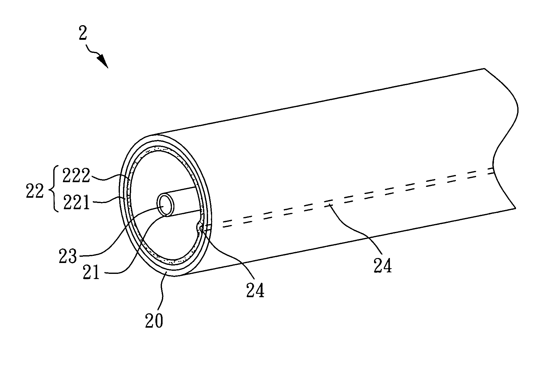
[0009]The present invention provides a field emission lamp comprising: a lamp-tube; an anode forming on the inner wall of the lamp-tube, the anode comprises a transparent conductive layer and a phosphor layer, and the transparent conductive layer locates between the inner wall of the lamp-tube and the phosphor layer; at least one auxiliary electrode; a cathode locating in the lamp-tube; and an emitter layer locating at the surface of the cathode. Preferably, the auxiliary electrode may locate between the transparent conductive layer and the phosphor layer, or locate between the transparent conductive layer and the inner wall of the lamp-tube. The transparent conductive layer is made of ITO (indium tin oxide), IZO (indium zinc oxide), AZO (aluminum doped zinc oxide), GZO (gallium doped zinc oxide), zinc oxide, or the combination thereof, and preferably the transparent conductive layer is made of ITO (indium tin oxide) to enhance a better light transmittance. The cathode can be made of any material that is used in a conventional field emission lamp such as metal, metal covered with CNT (carbon nanotube), or alloy (such as Ni / Au alloy) covered with carbon film. The auxiliary electrode of the present invention is helpful for shortening the electron transportation path length, and therefore the transportation efficiency of the electrons can be enhanced. Since the auxiliary electrode of the present invention can properly transfer the electrons accumulated in the phosphor layer, with the usage of the auxiliary electrode of the present invention, the phenomenon of micro electrical discharges caused by electron accumulation can be reduced, the voltage loss can be reduced, the temperature increase of the phosphor layer can be reduced, and therefore the lifetime of the field emission lamp can be elongated.
[0010]According to the field emission lamp of the present invention, the auxiliary electrode is preferably made in a linear form, a net form, a helix form, a ring form, or in a form comprising at least two selected from the group consisting of: a linear form, a helix form, and a ring form. The auxiliary electrode can be made in various forms to be randomly distributed in the lamp tube, and therefore can uniformly and efficiently evacuate the electron accumulation.
[0019]According to the method of fabricating a field emission lamp of the present invention, in the step (S1), the transparent conductive layer is preferably made of ITO (indium tin oxide). Generally, ITO film has a higher electrical conductivity than CNT (carbon nanotube) film. Based upon the same light transmittance, an ITO film has a higher electrical conductivity than a CNT film. In detail, when someone wants to increase the electrical conductivity of the CNT transparent conductive layer, it will be obtained by increasing the concentration of the CNT solution (i.e. the paste) of the conductive layer in the process of depositing the CNT solution on the inner wall of the lamp tube. However, when the concentration of the CNT solution is increased, the light transmittance of the CNT transparent conductive layer may decrease. Besides, in a conventional method of fabricating a field emission lamp, an inert gas such as nitrogen gas is required in the manufacturing of the CNT transparent conductive layer, in order to prevent the CNT transparent conductive layer from becoming decomposed during the sintering process of the phosphor layer. In contrast, in the method of fabricating a field emission lamp of the present invention, inert gas is not needed because the ITO transparent conductive layer can be heated with the phosphor layer and remains undamaged in the air. Therefore, the cost for manufacturing the field emission lamp can be reduced. Besides, when the ITO transparent conductive layer is heated with the phosphor layer, the phosphor paste provides oxygen vacancy, the resistance of the ITO transparent conductive layer is lowered, and therefore the electric conductivity of the ITO transparent conductive layer is increased.
[0020]According to the method of fabricating a field emission lamp of the present invention, the ITO transparent conductive layer is preferably made by the following steps: (A) filling the lamp-tube with an ITO solution; (B) draining the ITO solution from the lamp-tube and leaving an ITO thin film on the inner surface of the lamp-tube; and (C) heating the lamp-tube with the ITO thin film formed on the inner surface thereof. In a conventional method, an ITO transparent conductive layer is made by a physical vapor deposition method which applies high voltage to the target (sputtering material) under a vacuum circumstance, impacting the target (sputtering material) with the ionized inert gas to generate small particles, following with depositing those generated particles on the substrate. However, the cost involved is high and the thickness uniformity of the ITO transparent conductive layer cannot be satisfactory when a lamp tube is applied for functioning as the substrate. In contrast, the ITO transparent conductive layer of the present invention is fabricated by forming an ITO solution thin film on the inner surface of the lamp-tube following with a heating process, wherein the equipment used is inexpensive and therefore the cost involved can be lowered. The ITO transparent conductive layer formed by the method of the present invention has excellent thickness uniformity and high strength that enables the formed ITO transparent conductive layer not to be fragile.
[0021]According to the method of fabricating a field emission lamp of the present invention, the auxiliary electrode is preferably made in a linear form, a net form, a helix form, a ring form, or in a form comprising at least two selected from the group consisting of: a linear form, a helix form, and a ring form. The auxiliary electrode can be made in various forms to be randomly distributed in the lamp tube, and therefore can uniformly and efficiently evacuate the electron accumulation.

Problems solved by technology

Though fluorescent lamps are advantageous in high brightness, the mercury vapor therein threatens the health of human beings since fractures or leakage of the tube result in the release of toxic mercury vapor.
However, the light transmittance of the CNT transparent conductive layer may decrease with the increasing of the concentration of the CNT solution.
Besides, an inert gas such as nitrogen gas is required at the manufacturing of the CNT transparent conductive layer to prevent the CNT transparent conductive layer becoming decomposed during the sintering process of the phosphor layer, and therefore a high manufacturing cost will be incurred.
Such cases may result in short lifetime and low luminous efficacy of the field emission lamp.

Method used


Image

  • Field emission lamp and method for making the same
  • Field emission lamp and method for making the same
  • Field emission lamp and method for making the same

Examples


example 1

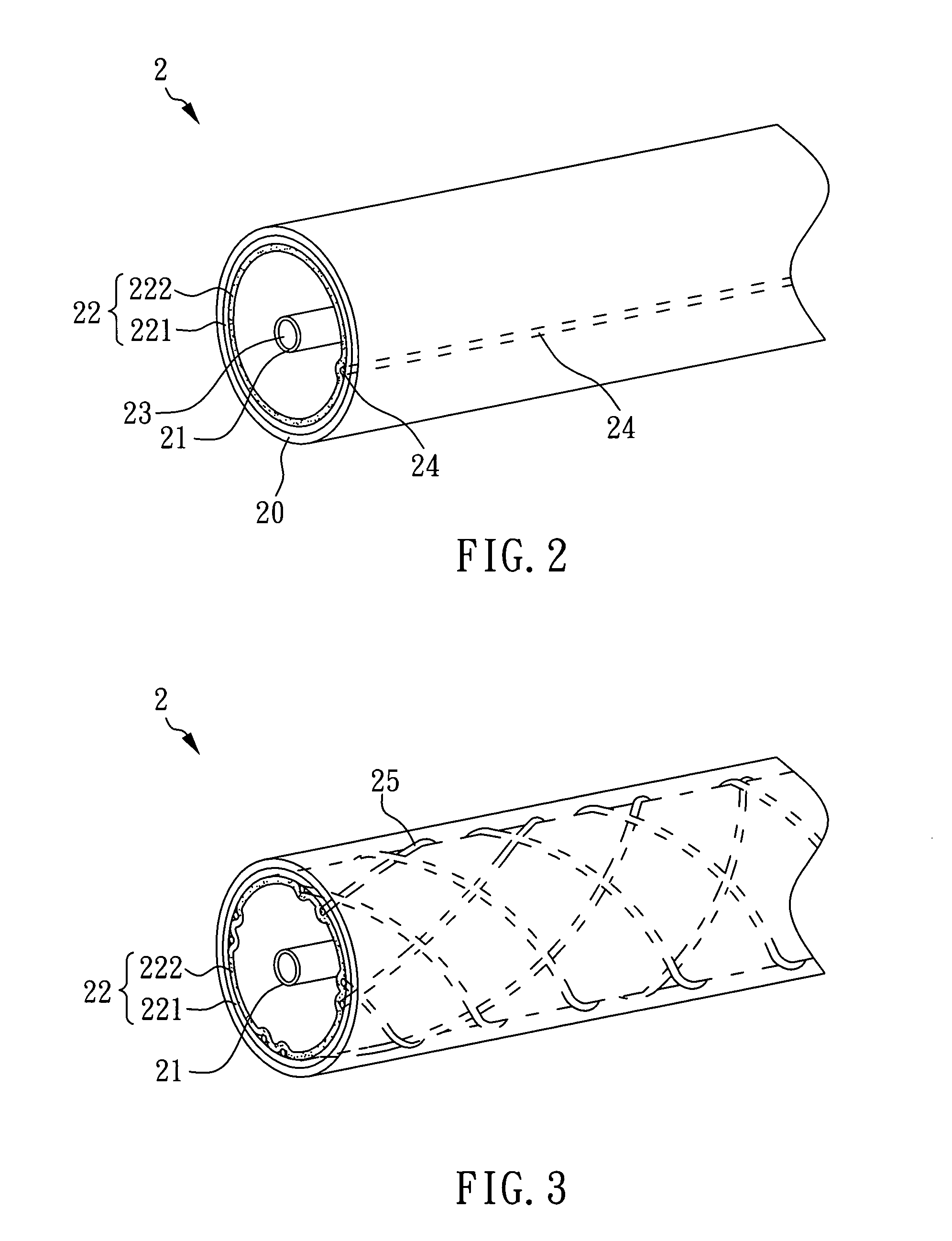
[0035]With reference to FIG. 2, there is shown a field emission lamp of the present example 1, which comprises a lamp-tube 20, an anode 22, an auxiliary electrode 24, a cathode 23, and an emitter layer 21. The anode 22 forms on the inner wall of the lamp-tube 20 and comprises a transparent conductive layer 221 and a phosphor layer 222. The transparent conductive layer 221 is made of ITO (indium tin oxide) to enhance high light-transmittance. The auxiliary electrode 24 is in a linear form and locates between the transparent conductive layer 221 and the phosphor layer 222. The auxiliary electrode 24 is made of silver and the line width of the auxiliary electrode is 500 μm. The cathode 23 locates in center of the lamp-tube 20 and is a nickel-chromium alloy wire. The emitter layer 21 locates on the surface of the cathode 23 and is made of CNT (carbon nanotube).

[0036]The auxiliary electrode 24 is helpful for shortening the electron transportation path length, and therefore the transporta...

example 2

[0037]With reference to FIG. 3, there is shown a field emission lamp of the present example 2. Except that the auxiliary electrode 25 is in a net form, the material of the emitter layer 21 is diamond-like carbon instead of CNT, and the material of the auxiliary electrode 25 is copper, the field emission lamp of the present example 2 is the same as that described in the example 1.

example 3

[0038]With reference to FIG. 4, there is shown a field emission lamp of the present example 3. Except that the auxiliary electrode 26 is in a helix form, the material of the emitter layer 21 is nano-diamond instead of CNT, and the material of the auxiliary electrode 26 is nickel, the field emission lamp of the present example 3 is the same as that of the example 1.


PUM


Abstract

A field emission lamp and method of fabricating the same are disclosed, the field emission lamp of the present invention comprising a lamp tube, an anode, at least one auxiliary electrode, a cathode, and an emitter layer. The anode comprises a transparent conductive layer and a phosphor layer, and the transparent conductive layer is made of ITO, IZO, AZO, GZO, zinc oxide, or the combination thereof. The auxiliary electrode of the field emission lamp of the present invention can shorten the electron transportation path length, increase the electron transportation efficiency, reduce the phenomenon of micro-discharges caused by electron charging, reduce the voltage loss, reduce the temperature increase of the phosphor layer and elongate the lifetime of the field emission lamp.

Description

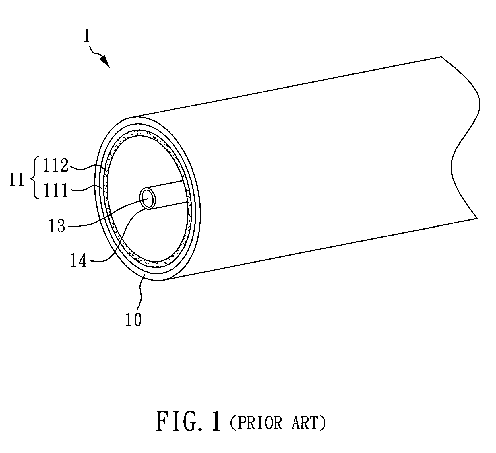
BACKGROUND OF THE INVENTION[0001]1. Field of the Invention[0002]The present invention relates to a field emission lamp and a method for making the same.[0003]2. Description of Related Art[0004]Fluorescent lamps widely used for illumination usually contain a transparent glass tube coated with fluorescent materials on their inner walls, and a mercury vapor filled in the transparent glass tube. Though fluorescent lamps are advantageous in high brightness, the mercury vapor therein threatens the health of human beings since fractures or leakage of the tube result in the release of toxic mercury vapor.[0005]Therefore, a novel field emission lamp without the usage of mercury vapor has been developed, as illustrated in FIG. 1, which comprises: a transparent glass tube 10, an anode 11, a cathode 13, and a field emission layer 14, in which the anode 11 comprises a transparent conductive layer 111 and a phosphor layer 112.[0006]In a conventional field emission lamp, the transparent conductive...

Claims


Application Information

Patent Timeline
IPC IPC(8): H01J19/32H01J9/00
CPCH01J63/02H01J61/0672
Inventor YANG, TZUNG-HANDAI, BING-DA
Owner TATUNG COMPANY
Learn More