Semiconductor light emitting diode and method for manufacturing the same
a technology of semiconductor led and light-emitting diodes, which is applied in the direction of semiconductor/solid-state device manufacturing, semiconductor devices, electrical apparatus, etc., can solve the problems of reduced recombination efficiency, low efficiency of semiconductor led, and increased led price, so as to reduce or suppress the bad effect , the effect of reducing the bad
- Summary
- Abstract
- Description
- Claims
- Application Information
AI Technical Summary
Benefits of technology
Problems solved by technology
Method used
Image
Examples
first embodiment
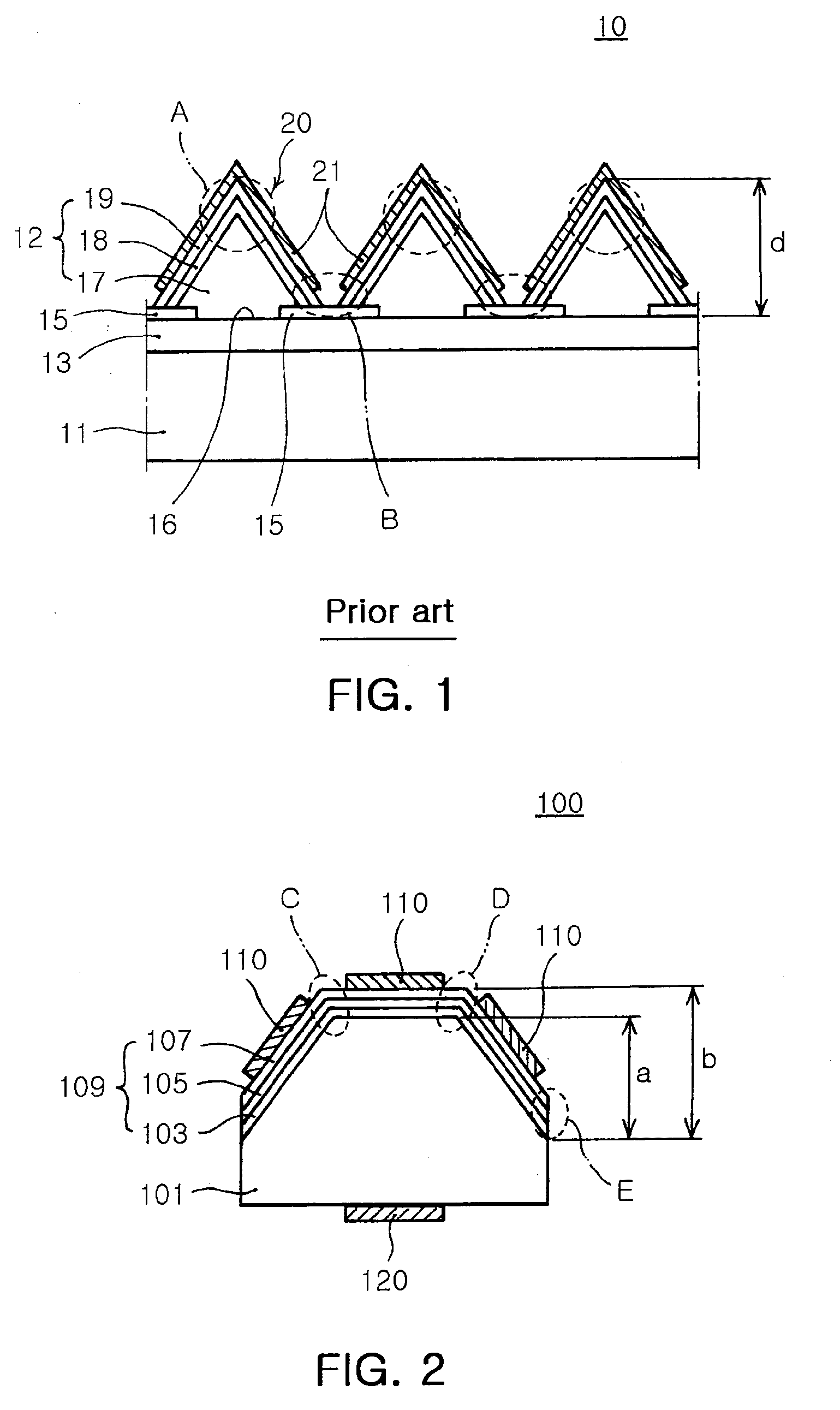
[0042]FIG. 2 is a sectional view of a semiconductor LED according to the present invention.
[0043]Referring to FIG. 2, the semiconductor LED 100 according to the first embodiment of the present invention includes a GaN-based substrate 101 and a light-emitting stack structure 109 formed on the GaN-based substrate 101. The GaN-based substrate 101 has a top surface having a three-dimensional shape. Specifically, the GaN-based substrate 101 is formed in a trapezoidal pyramid shape. The light-emitting stack structure 109 includes an n-type nitride semiconductor layer 103, an active layer 105, and a p-type nitride semiconductor layer 107, which are sequentially formed on the substrate 101.
[0044]A p-electrode 110 is formed on the p-type nitride semiconductor layer 107, and an n-electrode is formed on the bottom surface of the substrate 101. Preferably, the bottom surface of the substrate 101 becomes a light exit surface.
[0045]Therefore, the p-electrode 110 may include an ohmic-contact metal...
second embodiment
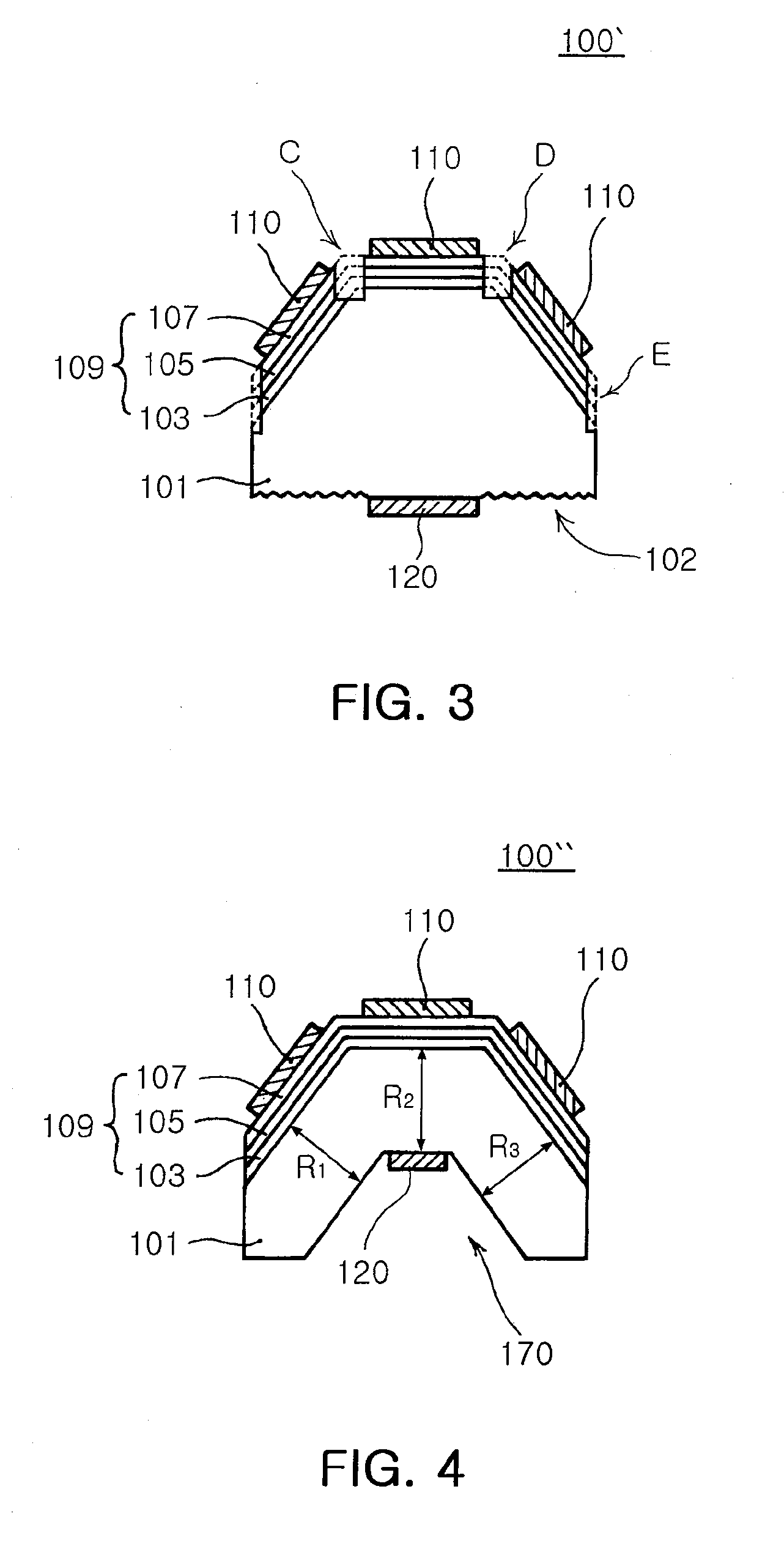
[0053]FIG. 3 is a sectional view of a semiconductor LED according to the present invention. In the semiconductor LED 100′ of FIG. 3, edges C, D and E of a three-dimensional light-emitting stack structure are removed using an etching process. By removing the edges C,
[0054]D and E, a large amount of crystal defect existing in the edges is also removed. Thus, the bad effect caused by the crystal defect can be reduced or suppressed. A passivation layer (150 in FIG. 12) may be formed at the regions where the edges C, D and E are removed. The passivation layer may be formed of insulating material such as SiO2. The passivation layer can prevent the p-electrode 110 and the active layer 105 from being directly contacted with each other and can interrupt a undesired current flowing through the edges C, D and E.
[0055]The GaN-based substrate 101 may have an uneven bottom surface 102, which is a light exit surface. The uneven bottom surface 102 provides a roughness. The uneven bottom surface 102...
third embodiment
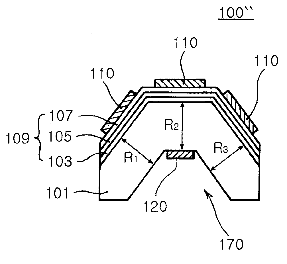
[0056]FIG. 4 is a sectional view of a semiconductor LED according to the present invention. In the semiconductor LED 100″ of FIG. 4, a groove 170 is formed in a bottom surface of a substrate 101. The groove 170 reduces a deviation of thickness R1, R2 and R3 of the substrate 101. Because a deviation of current paths passing through the substrate 101 is reduced, the current can flow more uniformly. Consequently, the operating voltage is lowered and a local concentration of the current density can be prevented. That is, the groove 170 formed in the bottom surface of the substrate 101 functions to accelerate a current diffusion. The semiconductor LED 100″ also has the above-described advantages.
[0057]FIG. 5 is a sectional view of a semiconductor LED according to a fourth embodiment of the present invention. Referring to FIG. 5, a groove 170 is formed in a bottom surface of a substrate 101 so as to reduce a thickness deviation of the substrate 101. Also, the substrate 101 has an uneven b...
PUM
 Abstract
Description
Claims
Application Information
 - R&D
- Intellectual Property
- Life Sciences
- Materials
- Tech Scout
- Unparalleled Data Quality
- Higher Quality Content
- 60% Fewer Hallucinations
Browse by: Latest US Patents, China's latest patents, Technical Efficacy Thesaurus, Application Domain, Technology Topic, Popular Technical Reports.
© 2025 PatSnap. All rights reserved.Legal|Privacy policy|Modern Slavery Act Transparency Statement|Sitemap|About US| Contact US: help@patsnap.com


