Integrated semiconductor light-emitting device and its manufacturing method
a semiconductor and light-emitting device technology, applied in semiconductor/solid-state device manufacturing, semiconductor devices, electrical appliances, etc., can solve the problems of extreme reduction of an emission intensity only in that area, inability to control an etching shape, and inability to exhibit uniform emission intensity over the whole element, etc., to achieve excellent in-plane emission intensity, high emission intensity, and high in-plane uniformity
- Summary
- Abstract
- Description
- Claims
- Application Information
AI Technical Summary
Benefits of technology
Problems solved by technology
Method used
Image

Examples
example
[0881]There will be described the present invention with reference to examples. Materials, amounts, proportions, specific processes and process orders in the following examples may be appropriately modified without departing from the scope of the invention. The scope of this invention should not be interpreted to be limited to the specific examples described below. Furthermore, in the drawings referred in the following examples, some sizes are deliberately changed to help understanding the structures, but practical dimensions are as indicated in the following description.
Examples of the Invention in Relation to Section A
example a-1
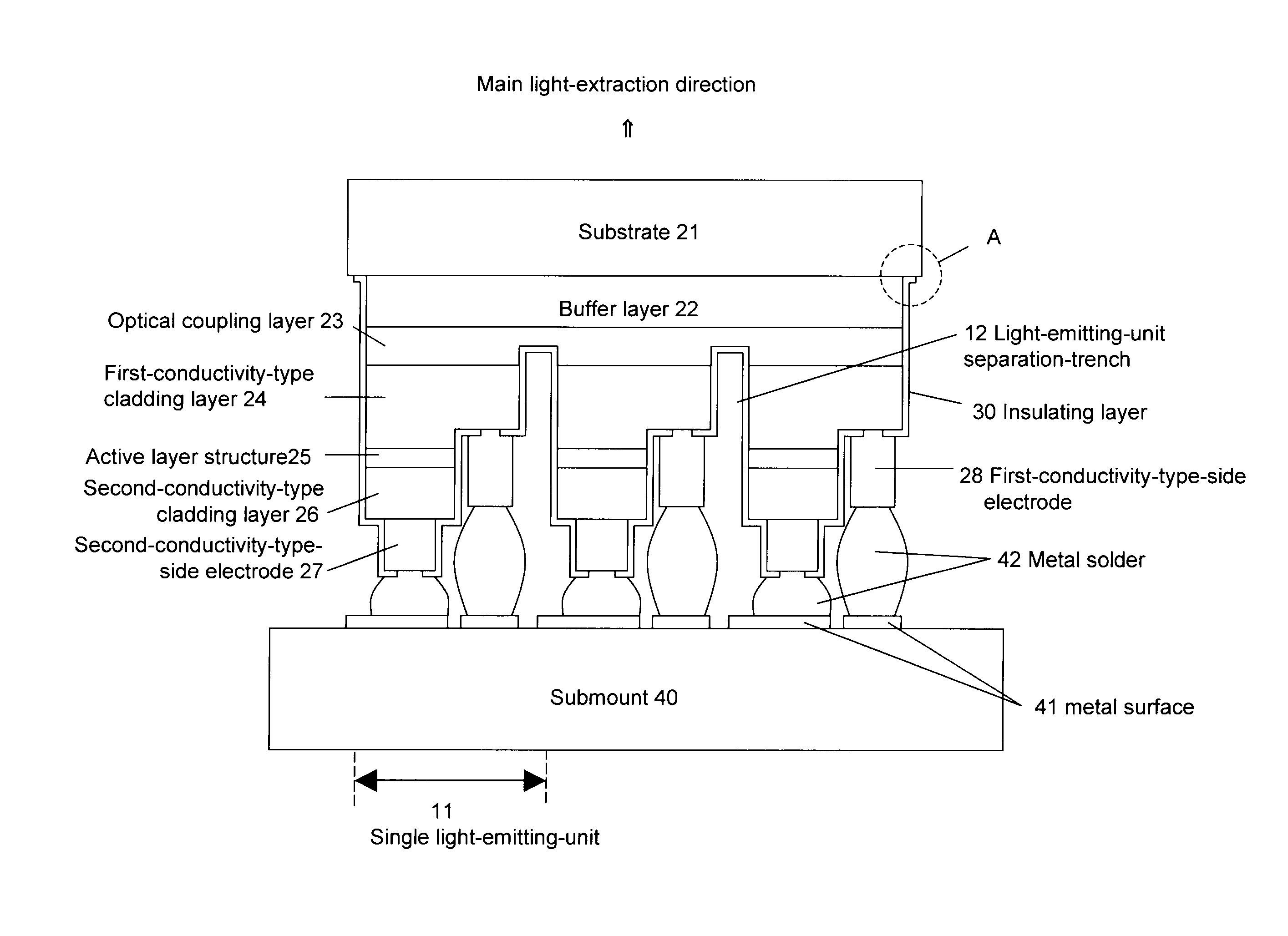
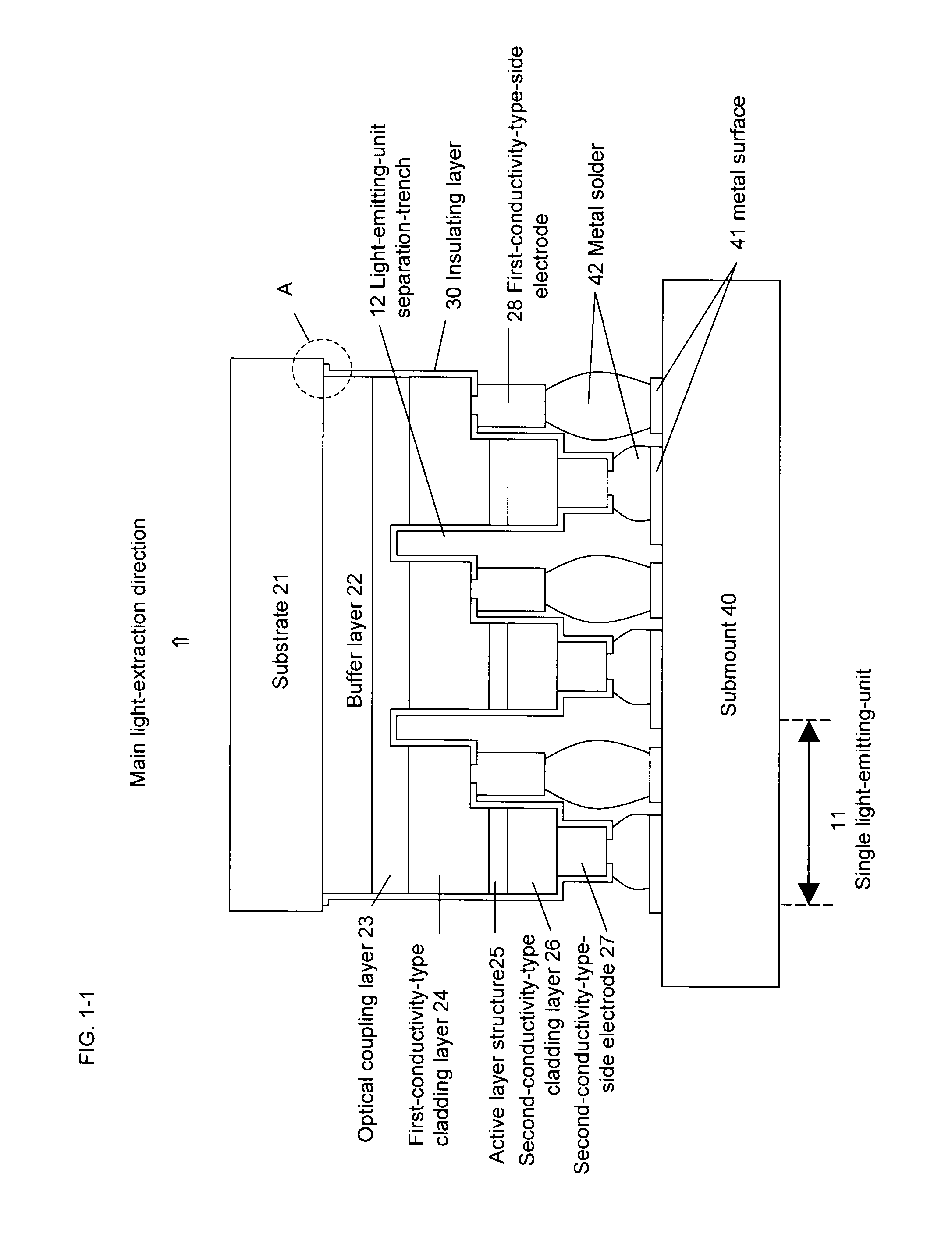
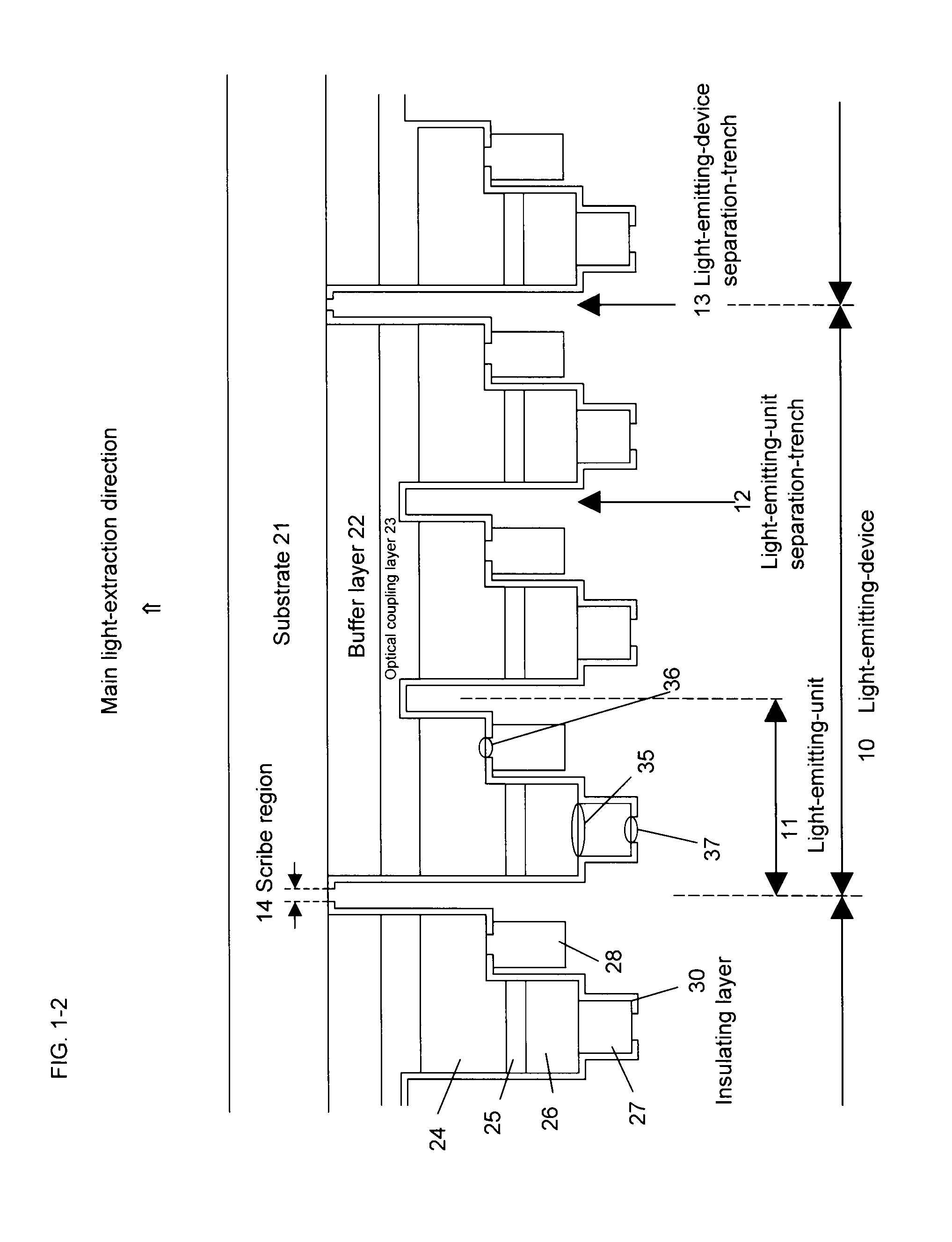
[0882]The light-emitting-device shown in FIG. 1-15 was manufactured by the following procedure. FIGS. 1-6 to 10, 12 and 14 will be referred to as a related process drawing.
[0883]First was prepared a c+ plane sapphire substrate 21 with a thickness of 430 μm, on which an undoped GaN layer with a thickness of 10 nm was formed by growing at a low temperature by MOCVD as a first buffer layer 22a; and then an undoped GaN layer with a thickness of 0.5 μm and a Si-doped (Si concentration: 7×1017 cm−3) GaN layer with a thickness of 0.5 μm were deposited at 1040° C. as a second buffer layer 22b with a thickness of 1 μm. Subsequently, an undoped GaN layer with a thickness of 3.5 μm was formed at 1035° C. as an optical coupling layer 23.
[0884]Then, a Si-doped (Si concentration: 1×1018 cm−3) GaN layer was formed to 2 μm as a first-conductivity-type (n-type) second cladding layer 24b; a Si-doped (Si concentration: 3×1018 cm−3) GaN layer was formed to 0.5 μm as a first-conductivity-type (n-type) c...
example a-2
[0903]The procedure in Example A-1 was repeated, except that after depositing the optical coupling layer 23, a thin-film crystal layer was deposited as described below. Specifically, an undoped GaN was formed at 1035° C. to a thickness of 3.5 μm as an optical coupling layer 23 as described in Example A-1, and then a Si-doped (Si concentration: 5×1018 cm−3) GaN layer was formed to 4 μm as a first-conductivity-type (n-type) second cladding layer 24b; a Si-doped (Si concentration: 8×1018 cm−3) GaN layer was formed to 0.5 μm as a first-conductivity-type (n-type) contact layer 24c; and then a Si-doped (Si concentration: 5.0×1018 cm−3) Al0.10Ga0.90N layer was formed to 0.1 μm as a first-conductivity-type (n-type) first cladding layer 24a. Then, an active layer structure 25 were formed by depositing alternately undoped GaN layer to a thickness of 13 nm at 850° C. as a barrier layer and undoped In0.1Ga0.9N layer to a thickness of 2 nm at 720° C. as a quantum well layer such that eight quant...
PUM
 Abstract
Description
Claims
Application Information
 - R&D
- Intellectual Property
- Life Sciences
- Materials
- Tech Scout
- Unparalleled Data Quality
- Higher Quality Content
- 60% Fewer Hallucinations
Browse by: Latest US Patents, China's latest patents, Technical Efficacy Thesaurus, Application Domain, Technology Topic, Popular Technical Reports.
© 2025 PatSnap. All rights reserved.Legal|Privacy policy|Modern Slavery Act Transparency Statement|Sitemap|About US| Contact US: help@patsnap.com