
Optical sensor for measuring emission light from an analyte

Inactive Publication Date: 2010-12-23
KONINKLIJKE PHILIPS ELECTRONICS NV
View PDF4 Cites 24 Cited by
  • Summary
  • Abstract
  • Description
  • Claims
  • Application Information

AI Technical Summary

Benefits of technology

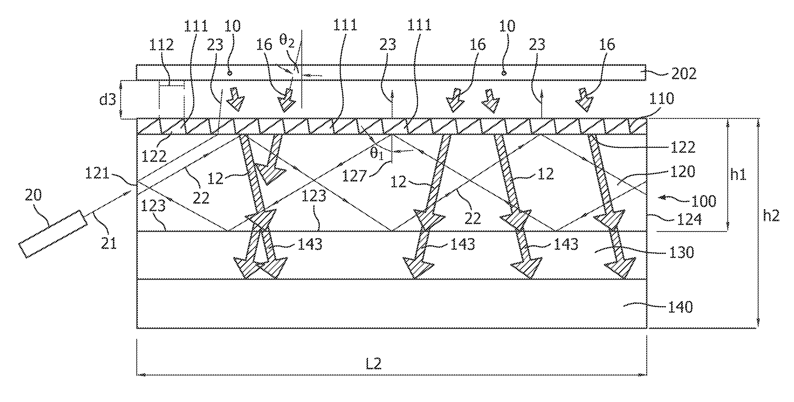
[0009]The current invention proposes in an embodiment the use of a waveguide, especially a substantially planar waveguide, where excitation light (wavelength λ) is coupled in from the side. The light is reflected at the top and bottom surface of the waveguide by total internal reflection. Furthermore the top surface of the waveguide may contain a diffraction grating such that the 1st order is coupled out along a direction (preferentially) substantially parallel to the surface normal, i.e. substantially perpendicular to the top surface. In this way, a substantially planar structure for coupling out light in a direction perpendicular to the planar object may be obtained.
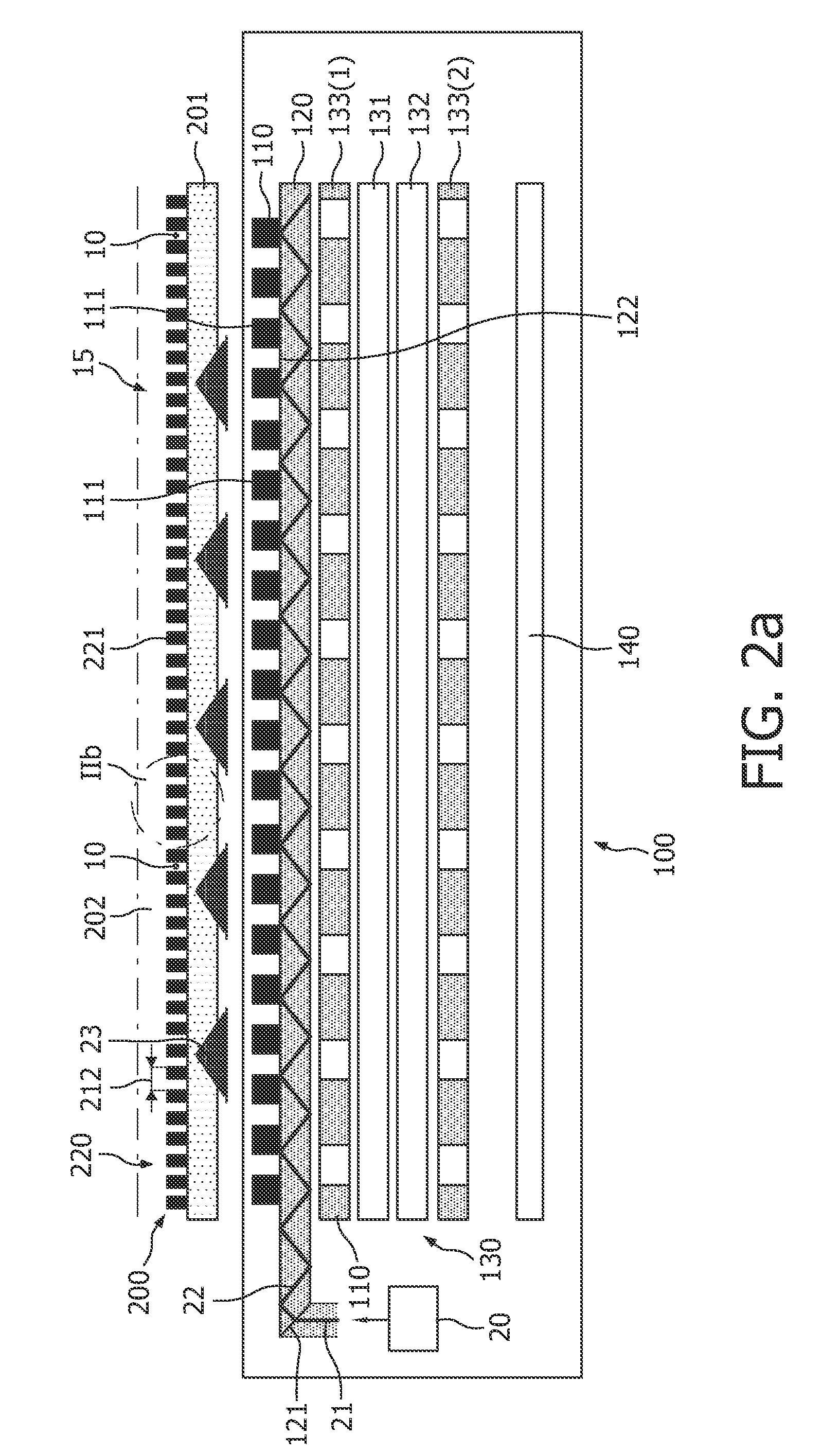
[0011]In this way all optical components, including detection optics, and optionally also including illumination optics, may be substantially planar in geometry and can be stacked easily on top of a 2D-sensor, resulting in a compact planar optical imaging device for reading an analyte, for instance on a wire-grid substrate.
[0018]In an embodiment, the sensor waveguide surface comprises a diffraction grating (also indicated as “grating” or “grating coupler”), wherein the diffraction grating is arranged to couple out excitation light with a predetermined wavelength in a first order diffraction substantially perpendicular to the sensor waveguide surface. In this way, outcoupling of light may be enabled and excitation light with a predetermined wavelength can be provided to the analyte. Further, in an embodiment, the diffraction grating is substantially transmissive for emission light with a predetermined wavelength, more especially for such emission perpendicular to the sensor waveguide surface. Since the grating may be blazed to the predetermined wavelength, and the emission of the analyte will in generally be (Stokes-) shifted relative to excitation light, the grating is on the one hand arranged to allow excitation light in first order, and substantially perpendicular to the sensor waveguide surface, escape from the waveguide, and on the other hand, arranged to allow emission light substantially unhindered enter the waveguide.
[0027]In a further specific embodiment, the light source is arranged to couple light source light into the waveguide, more especially, the light source and the waveguide are arranged to provide total internal reflection of the incoupled light source light. In an embodiment, the light source and the waveguide are arranged to provide incoupled light source light with an angle θ1 relative to a normal to the sensor waveguide surface in a typical range of about 70-80°. Especially under such condition, excitation light, especially in the range of about 550-700 nm, may be coupled out relatively efficiently in first order, while at the same time having a relatively high transmission for emission light of the analyte, especially in the range of about 650-900 nm, especially about 650-750 nm.

Problems solved by technology

A disadvantage of prior art sensors may be that such sensors are relatively bulky sensors.
Other disadvantages of the prior art may be necessity to use relatively complicated optical solutions to measure emission from analytes.

Method used


Image

  • Optical sensor for measuring emission light from an analyte
  • Optical sensor for measuring emission light from an analyte
  • Optical sensor for measuring emission light from an analyte

Examples


example

[0111]For a number of configurations, the optical properties of the specific optical sensor 100 were determined. For the sake of understanding, an example is given.

[0112]Using rigorous coupled wave calculations, a grating has been designed coupling out light at an excitation wavelength of 650 nm and transmitting light at an emission wavelength of 715 nm (10% red shift). A grating pitch of 450 nm has been used, the periodic structures having a saw-tooth (blazed) shape with a total height of 420 nm. It appears that for the indicated excitation wavelength around 9% of the light is coupled out in first order, whereas for the emission wavelength a transmission of 100% can be obtained for most entrance angles. For large entrance angles (larger than e.g. 10 degrees) the 0-order diffraction efficiency starts to decrease due to the appearance of higher order diffraction orders.

[0113]The term “substantially” herein, such as in “substantially all emission” or in “substantially consists”, will ...


PUM

PropertyMeasurementUnit
Nanoscale particle sizeaaaaaaaaaa
Wavelengthaaaaaaaaaa

Abstract

The invention provides an optical sensor (100). The optical sensor (100) comprises a planar waveguide (120) capable of emitting radiation (22) in a direction perpendicular to the sensor waveguide surface (122) and capable of accepting and transmitting radiation (16) to detector (140), preferably a planar detector (140). Further, optionally one or more lenses (133), one or more spectral filters (131) and one or more polarisation filters (132) may be arranged between the waveguide (120) and the detector (140). The optical sensor (100) is especially arranged to read out a wire grid substrate (200) with analytes (10).

Description

FIELD OF THE INVENTION[0001]The invention relates to an optical sensor for measuring emission light from an analyte as well as to a method for measuring emission light from the analyte with an optical sensor.BACKGROUND OF THE INVENTION[0002]Optical sensors, such as biosensors, for measuring quantitatively and / or qualitatively the presence of analytes are known in the art.[0003]WO 2006 / 136991 for instance discloses a qualitative or quantitative luminescence sensor, for example a biosensor or chemical sensor, using sub-wavelength aperture or slit structures, i.e. using apertures or slit structures having a smallest dimension smaller than the wavelength of the excitation radiation in the medium that fills the aperture or slit structure.[0004]The luminescence sensor system of WO 2006 / 136991 comprises a luminescence sensor, an excitation radiation source and a detector. The luminescence sensor comprises a substrate provided with at least one aperture or slit having a smallest dimension a...

Claims


Application Information

Patent Timeline
IPC IPC(8): H01J40/00G01N21/64
CPCG01N21/645G01N21/7703G01N21/648G01N21/6454
Inventor SCHLEIPEN, JOHANNES J.H.B.
Owner KONINKLIJKE PHILIPS ELECTRONICS NV
Learn More