
Molecular electronic device including organic dielectric thin film and method of fabricating the same

a technology of electronic devices and thin films, applied in solid-state devices, nanoinformatics, instruments, etc., can solve problems such as difficult commercialization of such electronic devices, and achieve the effect of preventing short circuits

Inactive Publication Date: 2010-11-25
ELECTRONICS & TELECOMM RES INST
View PDF5 Cites 2 Cited by
  • Summary
  • Abstract
  • Description
  • Claims
  • Application Information

AI Technical Summary

Benefits of technology

[0007]The present invention provides a molecular electronic device with a desired electronic characteristic by preventing short circuits, usually caused by penetration of an electrode material into a molecular active layer, when implementing an ultra-highly integrated nanoelectronic device including a miniaturized structure of several to several tens of nanometers that utilizes an electronic characteristic of the molecular active layer.
[0008]The present invention also provides a method of fabricating a molecular electronic device capable of improving yield and reliability of ultra-highly integrated nanoelectronic devices including a miniaturized structure of several to several tens of nanometers by preventing short circuits, usually caused by penetration of an electrode material into a molecular active layer when forming an electrode over the molecular active layer.
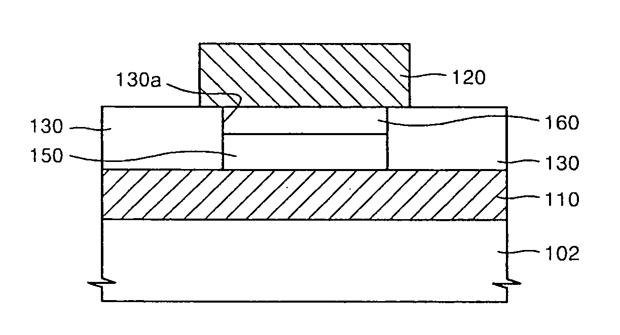
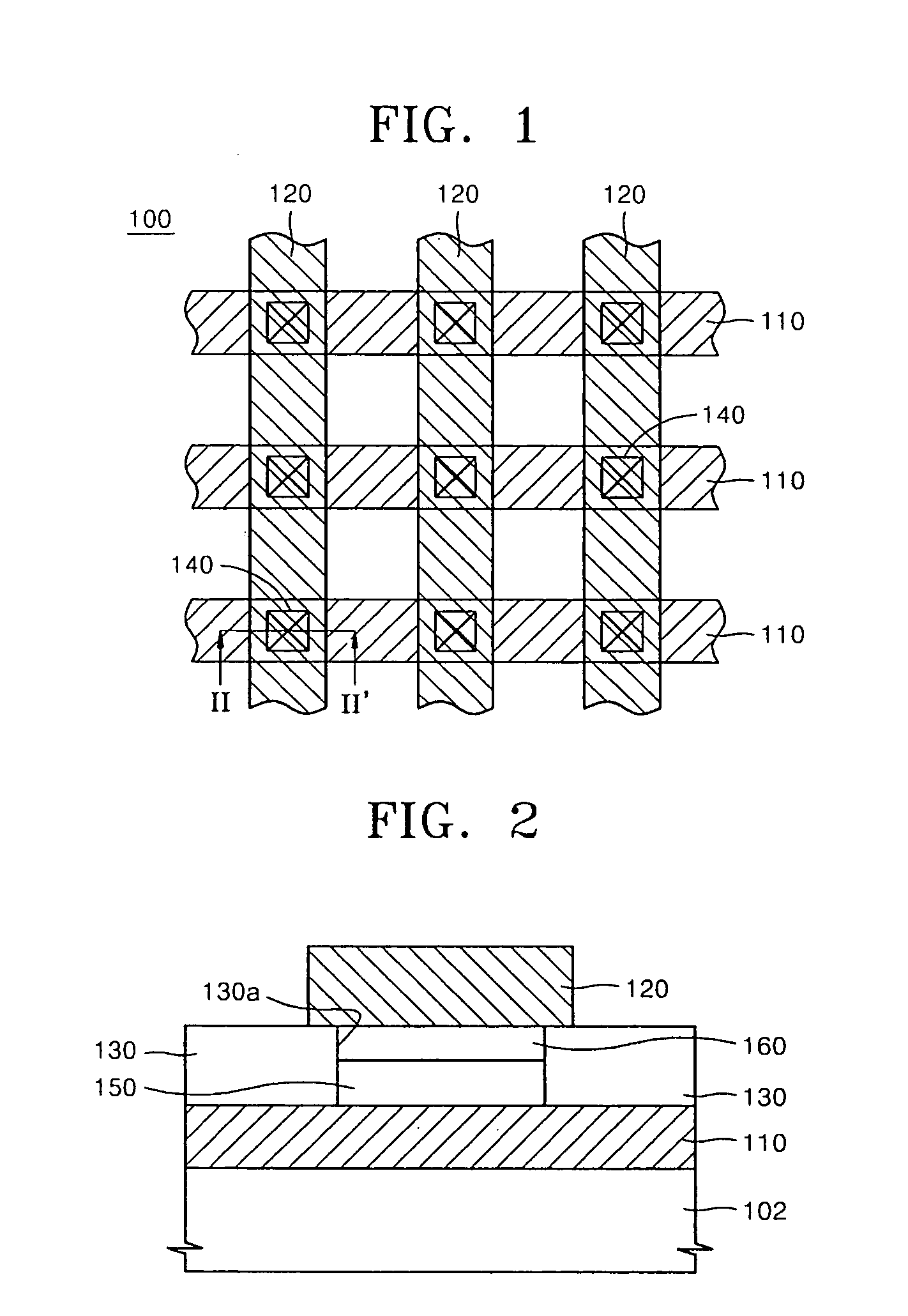
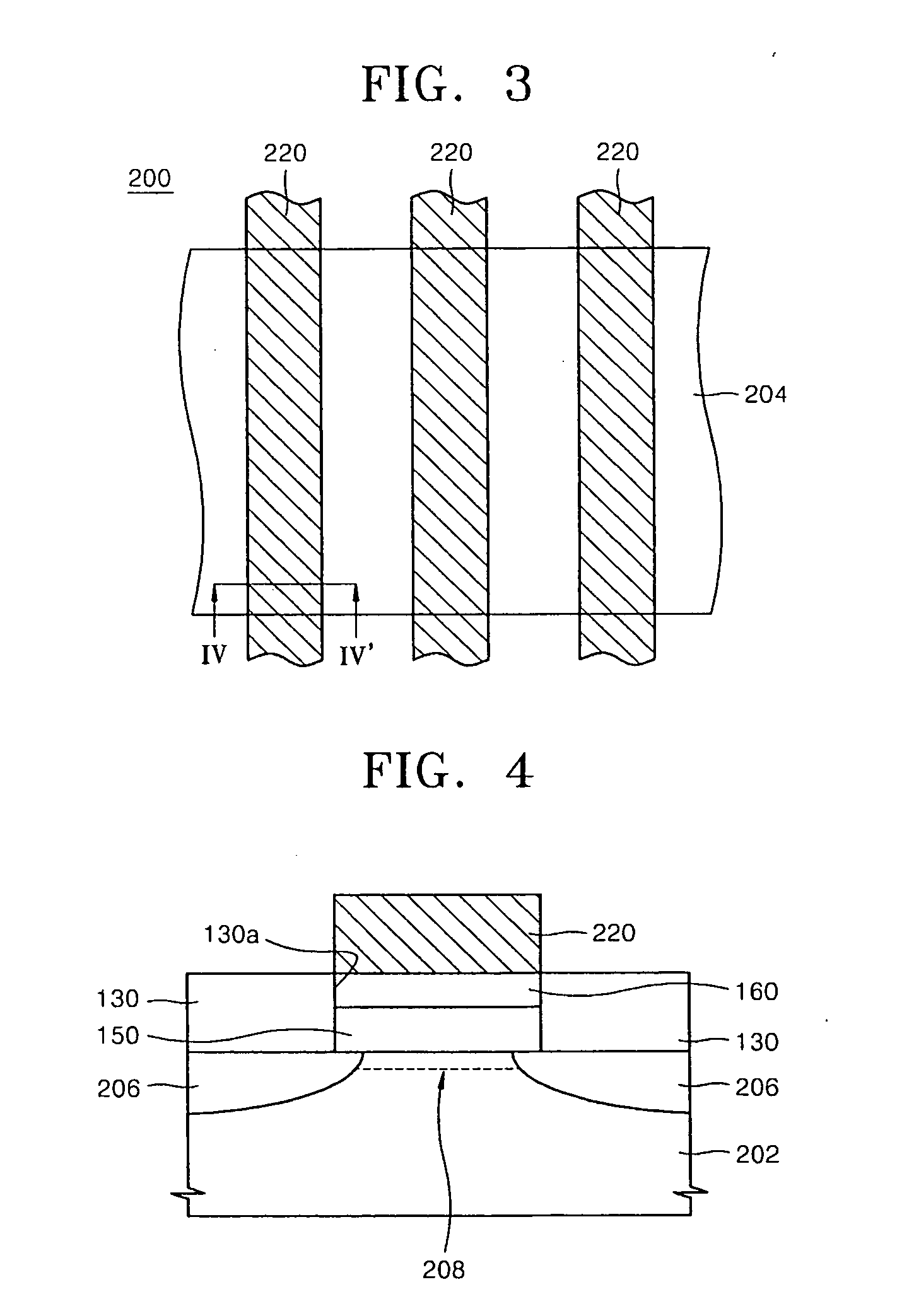
[0033]According to various exemplary embodiments of the present invention, when an electrode material is deposited over the molecular layer, even if the electrode material penetrates into the molecular active layer, the penetrated the electrode material cannot reach a bottom conductive layer since a distance from the molecular active layer to the bottom conductive layer increases due to the organic dielectric thin film formed between the molecular active layer and the bottom conductive layer. Therefore, the molecular electrode device according to the embodiments of the present invention can prevent an occurrence of short-circuit usually caused by the penetration of the electrode material into the molecular active layer. Accordingly, it is possible to improve yield and reliability of ultra-highly integrated nanoelectronic devices including a miniaturized structure with the size of several nanometers to several tens of nanometers.

Problems solved by technology

As a result, short circuits may occur in the molecular electronic device, and thus, the commercialization of such a molecular electronic device may be difficult.

Method used


Image

  • Molecular electronic device including organic dielectric thin film and method of fabricating the same
  • Molecular electronic device including organic dielectric thin film and method of fabricating the same
  • Molecular electronic device including organic dielectric thin film and method of fabricating the same

Examples


example 1

Fabrication of Molecular Electronic Device

[0110]A. Fabrication of Bottom Electrode and Organic Dielectric Thin Film

[0111]An insulation layer was formed on a silicon substrate. The insulation layer was formed of silicon oxide. A plurality of bottom electrodes were formed on the insulation layer. As similar to the bottom electrodes 110 illustrated in FIG. 1, the bottom electrodes were formed in line-type patterns. A line width of each of the bottom electrodes was about 50 nm. The bottom electrodes were formed by first coating a photoresist material on the insulation layer using a spin coating method and imprinting the photoresist material to form a mask pattern using a stamp. A Ti layer and an Au layer were sequentially deposited using an electron beam deposition method. The Ti layer and the Au layer were formed to thicknesses of about 5 nm and about 30 nm, respectively. The mask pattern was removed. In the current embodiment, the bottom electrodes were formed using a nano-imprinting ...

example 2

Verification of Self-Assembled Organic Dielectric Thin Film on Electrode

[0119]According to an embodiment of the present invention, when an organic dielectric thin film including amine alkylthiol-containing double molecular layers was formed on an electrode formed of Au, a sample including an Au layer was immersed into DMF solution to verify whether the organic dielectric thin film was formed on the surface of the Au layer (i.e., electrode). Amine alkylthiol (HS(CH2)11NH2) was injected into the DMF solution so that the concentration of amine alkylthiol was about 0.1 mM within the DMF solution, and a self-assembly rate of the amine alkylthiol on the surface of the Au layer was observed using a quartz crystal microbalance (QCM).

[0120]FIG. 8 illustrates a graph of amounts of the amine alkylthiol adsorbed onto the surface of the Au layer with respect to time using the QCM.

[0121]In FIG. 8, “I” indicates a moment at which the amine alkylthiol was injected into the DMF solution into which t...

example 3

Fabrication of Molecular Electronic Device Including Organic Dielectric Thin Film with Single Molecular Layer Structure

[0122]As comparison, an organic dielectric thin film with a single molecular layer was formed on an Au layer, and a molecular active layer chemically bound to the organic dielectric thin film to thereby fabricate a molecular electronic device. The organic dielectric thin film with the single molecular layer was obtained by self-assembling a compound of HS(CH2)2NH2 on the Au layer, and chemically binding an active material including a dying agent, such as Rose bengal, to the organic dielectric thin film so as to form the molecular active layer.


PUM


Abstract

Provided are a molecular electronic device and a method of fabricating the molecular electronic device. The molecular electronic device includes a substrate, an organic dielectric thin film formed over the substrate, a molecular active layer formed on the organic dielectric thin film and having a charge trap site, and an electrode formed on the molecular active layer. The organic dielectric thin film may be immobilized on the electrode or a Si layer by a self-assembled method. The organic dielectric thin film may include first and second molecular layers bound together through hydrogen bonds. An organic compound may be self-assembled over the substrate to form the organic dielectric thin film. The organic compound may include an M′-R-T structure, where M′, R and T represent a thiol or silane derivative, a saturated or unsaturated C1 to C20 hydrocarbon group which is substituted or unsubstituted with fluorine (F), and an amino(—NH2) or carboxyl (—COOH) group, respectively.

Description

CROSS-REFERENCE TO RELATED PATENT APPLICATION[0001]This application claims the benefits of Korean Patent Application No. 10-2006-0085375, filed on Sep. 5, 2006, and Korean Patent Application No. 10-2006-0103137, filed on Oct. 23, 2006, in the Korean Intellectual Property Office, the disclosures of which are incorporated herein in their entirety by reference.BACKGROUND OF THE INVENTION[0002]1. Field of the Invention[0003]The present invention relates to a molecular electronic device, and more particularly, to a molecular electronic device including a molecular active layer with a charge trap site and a method of fabricating the device.[0004]2. Description of the Related Art[0005]Much research has been dedicated to developing an organic semiconductor device using an organic material having π-electron conjugated bonds. Most of the attempts have been focused on electron transport characteristics of an organic layer interposed between two metal electrodes. Researchers have also attempted...

Claims


Application Information

Patent Timeline
Patent Type & Authority Applications(United States)
IPC IPC(8): H01L51/40
CPCB82Y10/00G11C11/14H01L51/0595H01L51/0073H01L27/285H10K19/202H10K85/6574H10K10/701
Inventor LEE, HYOYOUNGBANG, GYEONG SOOKPARK, JONGHYURKLEE, JUNGHYUNCHOI, NAK JINKOO, JA RYONG
Owner ELECTRONICS & TELECOMM RES INST
Learn More