Method for purifying silicon
a technology of silicon and purification method, applied in the direction of silicon compounds, crystal growth process, polycrystalline material growth, etc., can solve the problems of high processing difficulty and/or cost, and the process is very costly and capital-intensive way of producing silicon
- Summary
- Abstract
- Description
- Claims
- Application Information
AI Technical Summary
Benefits of technology
Problems solved by technology
Method used
Image
Examples
example 1
Methods of Purifying Silicon
[0089]Step A: Removal of P down to about 10 ppm
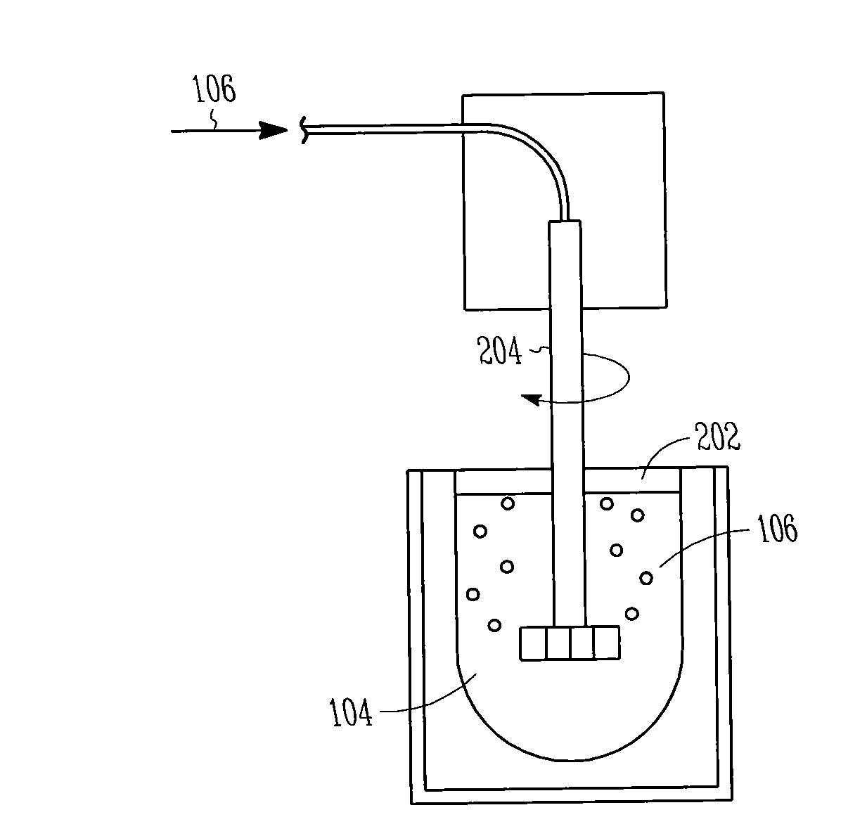
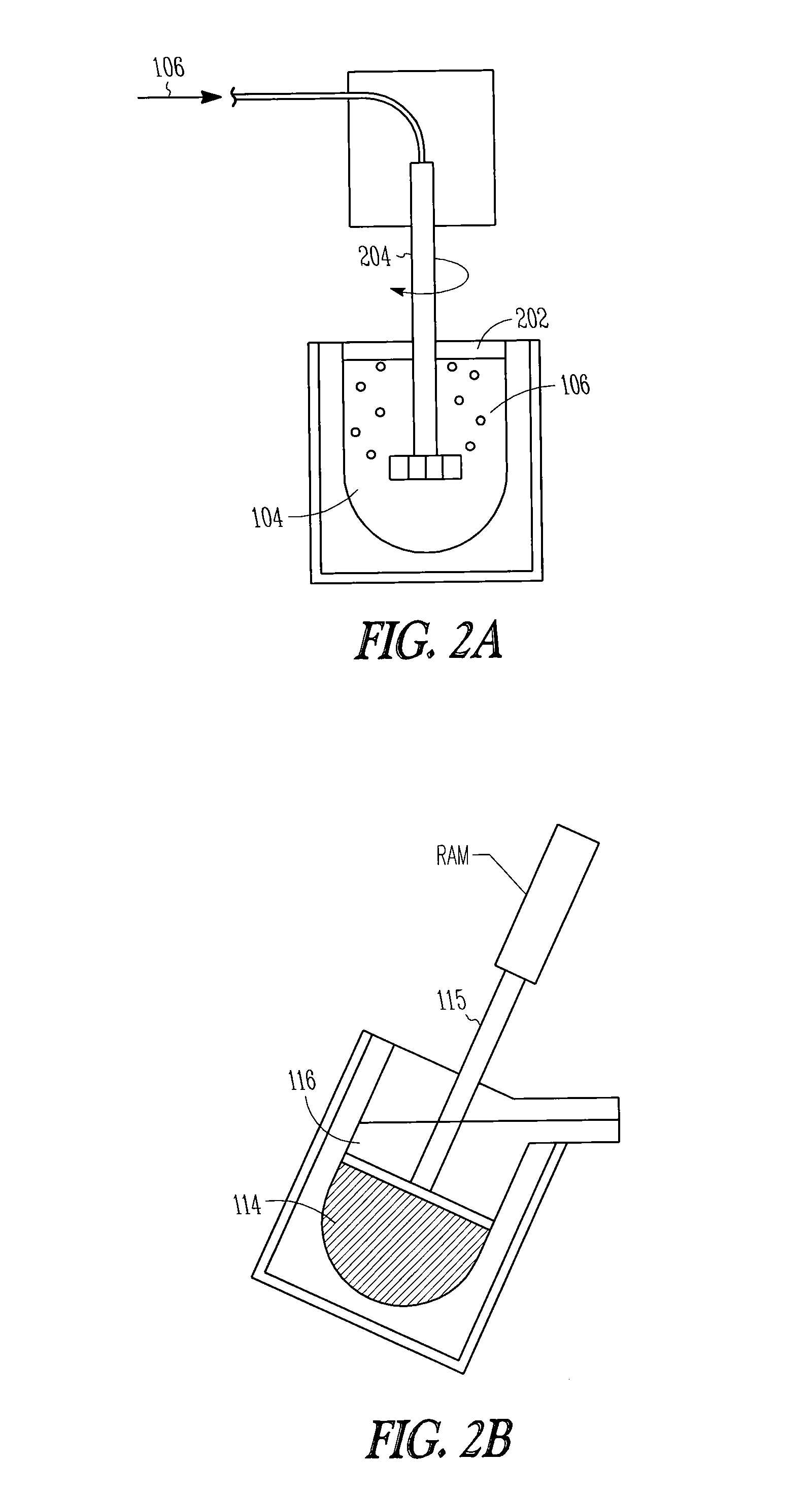
[0090]A 50-50 Al—Si mixture was melted by weight in an induction furnace until the mixture was completely molten at approximately 1000° C. A 1 / 3:1 / 3:1 / 3 mix of Cu:Al:Si also works well. The pure aluminium should have as low a phosphorous level as possible (e.g., about 1-10 ppm). The Cu should contain as low a phosphorous level (e.g., preferably less than about 30 ppm). Calcium can be added to help Ca3P4 precipitates form, if the metallurgical silicon is low in Calcium. This will make it easier for the phosphorous to be dragged by gas bubbles containing Cl2 and inert gas to the surface. A gas with about 4% Cl2 and 96% Argon was injected through a rotary impeller, spinning at about 800 RPM. The gas was injected for several hours until the phosphorous content was lowered to about 10 ppmw or low enough that the next step can reduce it to about 2 ppmw or less. Dross and salts were periodically scrimmed from the su...
example 2
[0097]The main difference between example 2 and example 1 is the injecting of gases and / or slagging of molten silicon first before adding of the solvent.
[0098]Step A) Injecting gases and mixing slag into the molten silicon. This step can lower the boron and phosphorous levels to acceptable levels so that steps C & D can further lower the phosphorous and boron concentrations to solar grade silicon levels. This step also lower elements like Ca, Mg, Al, Sr, Li, etc. which makes the directional solidification step easier.
[0099]Step B) Dissolving the Silicon in a solvent preferably aluminum, or aluminum and copper.
[0100]Step C) Use fractional crystallization to mechanically separate the majority of the solvent metal and silicon. The silicon crystals are formed by slowly cooling the molten mixture so that purified silicon crystals form. The silicon crystals can then be mechanically removed by several different possible methods. Preferable the crystals are separated with a tamp to hold the...
example 3
[0104]The main difference between example 3 and example 1 is the removal of step C directional solidification since injecting reactive gases such as oxygen can remove a solvent metal like aluminum as oxides.
[0105]I) Dissolving the Silicon in an solvent and injection gases or adding salts to remove impurities
[0106]II) Using fractional crystallization to mechanically separate the majority of the solvent metal and silicon.
[0107]III) Injecting gases and mixing slag into the molten silicon to remove impurities and solvent.
[0108]IV) Directional solidification / crystal pulling to form purified silicon using the Bridgeman, Float zone, Czochralski or other crystal growing processes.
PUM
| Property | Measurement | Unit |
|---|---|---|
| liquidus temperature | aaaaa | aaaaa |
| temperature | aaaaa | aaaaa |
| temperature | aaaaa | aaaaa |
Abstract
Description
Claims
Application Information
 - R&D
- Intellectual Property
- Life Sciences
- Materials
- Tech Scout
- Unparalleled Data Quality
- Higher Quality Content
- 60% Fewer Hallucinations
Browse by: Latest US Patents, China's latest patents, Technical Efficacy Thesaurus, Application Domain, Technology Topic, Popular Technical Reports.
© 2025 PatSnap. All rights reserved.Legal|Privacy policy|Modern Slavery Act Transparency Statement|Sitemap|About US| Contact US: help@patsnap.com


