
Semiconductor power module, inverter, and method of manufacturing a power module

a technology of semiconductor devices and power modules, which is applied in semiconductor devices, lighting and heating apparatus, cooling/ventilation/heating modifications, etc., can solve the problem of difficult to make all fins the same length on the base, and achieve the effect of preventing the bending of the base on the heat sink

Active Publication Date: 2010-08-19
HITACHI POWER SEMICON DEVICE
View PDF8 Cites 93 Cited by
  • Summary
  • Abstract
  • Description
  • Claims
  • Application Information

AI Technical Summary

Benefits of technology

[0012]In light of the above-mentioned technical problems, an object of the invention is to provide a semiconductor power module providing a fin-attached heat sink capable of making the length of pin fins even and preventing the bending of base, even though a forged fin-attached heat sink has a large sized base as large as 10 cm×10 cm or over, and a manufacturing method of the semiconductor power module, and also provide a power inverter using the semiconductor power module.
[0016]According to the invention, the length of pin fins can be made even on the forged heat sink used for the semiconductor power module in the power inverter, and the bending of the base on the heat sink can be made prevented.

Problems solved by technology

Therefore, it is difficult to make the all fins the same length on the base.

Method used


Image

  • Semiconductor power module, inverter, and method of manufacturing a power module
  • Semiconductor power module, inverter, and method of manufacturing a power module
  • Semiconductor power module, inverter, and method of manufacturing a power module

Examples


Embodiment Construction

[0031]Hereinafter, an embodiment of the invention will be described with reference to the drawings.

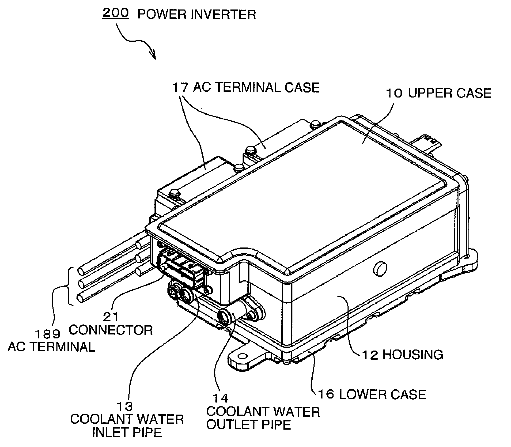
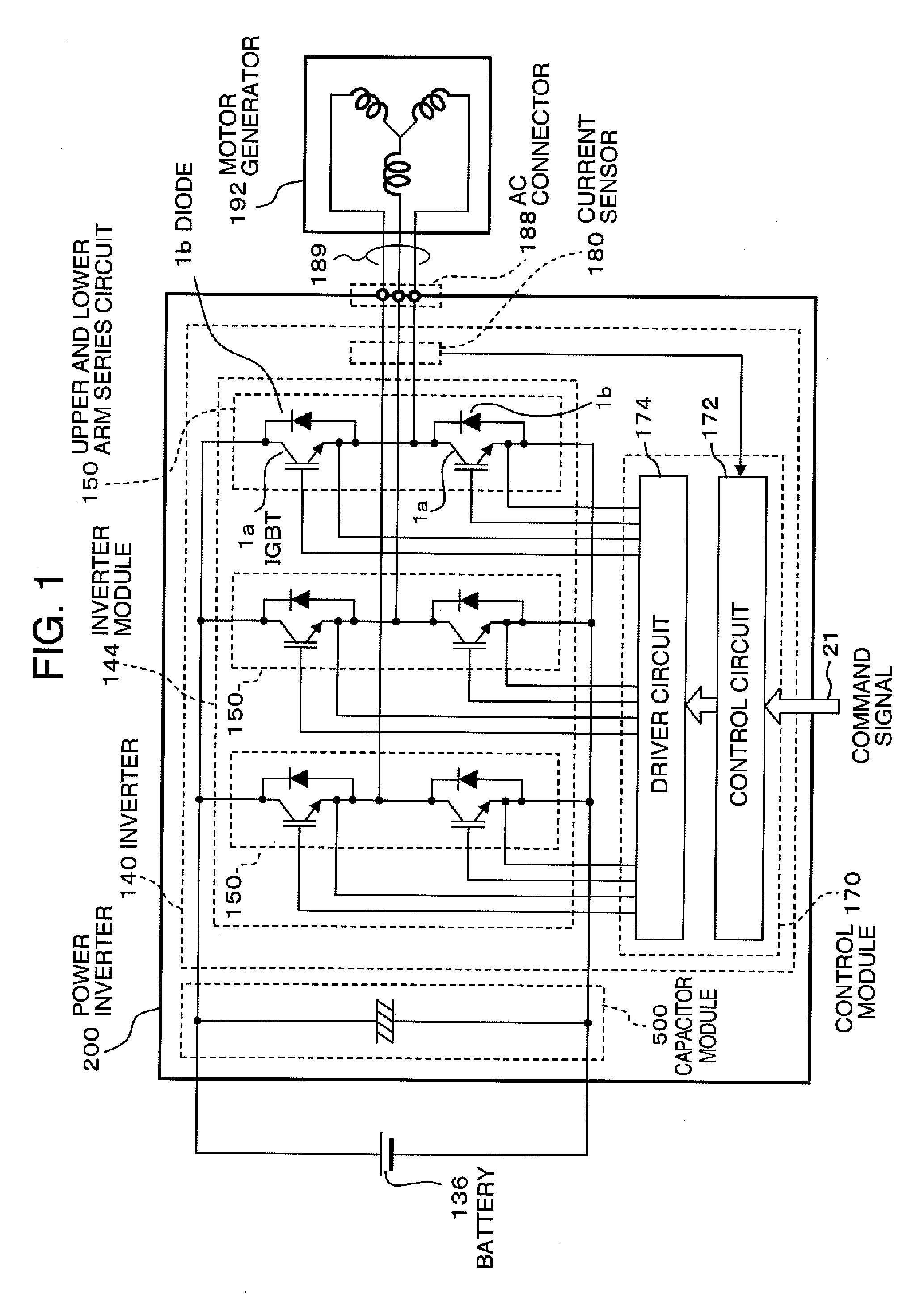
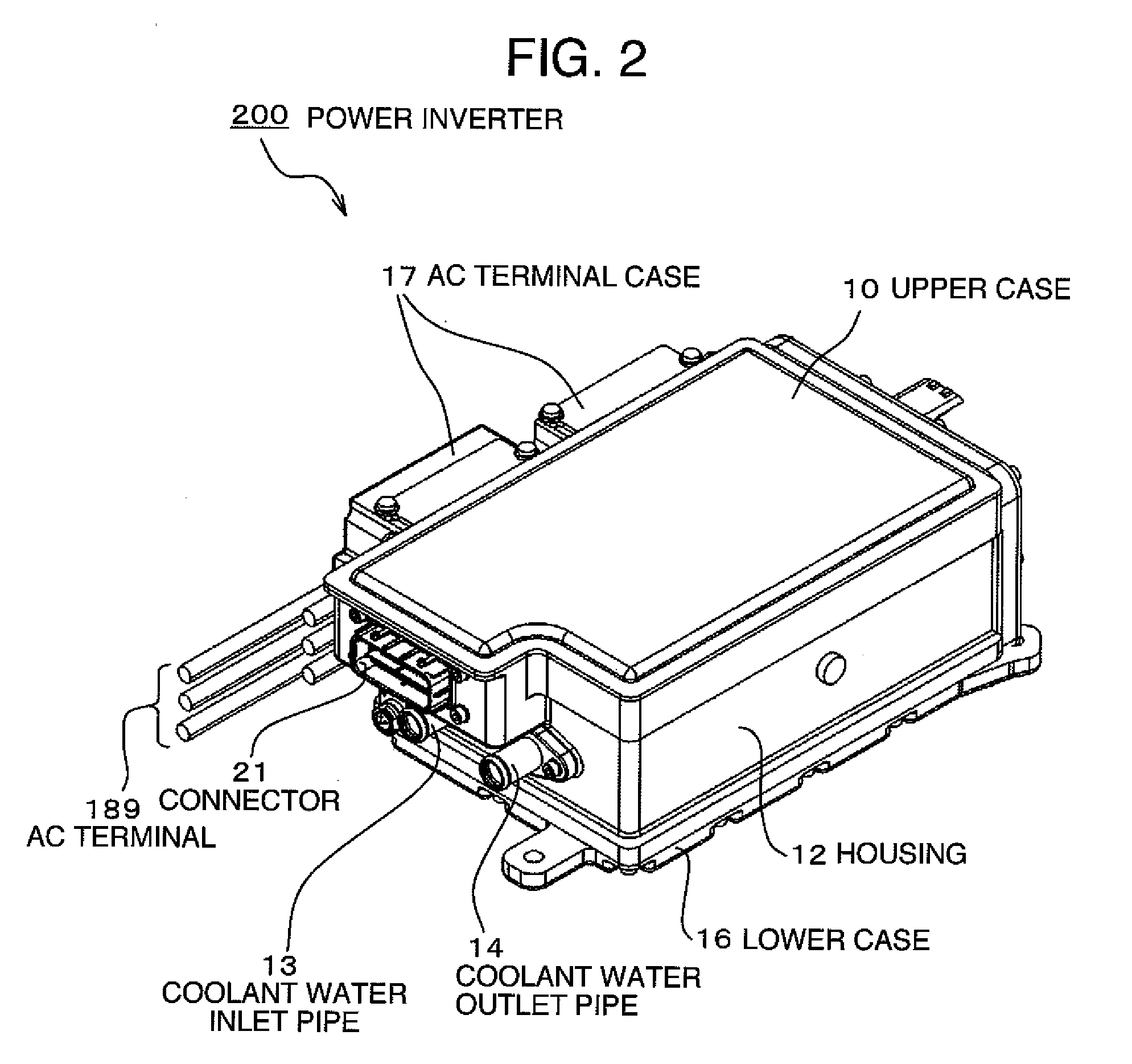
[0032]FIG. 1 is a diagram showing a circuit block configuration, as an example, of a power inverter in the embodiment of the invention. As shown in FIG. 1, a power inverter 200 is connected with a battery 136 and a motor generator 192 to convert a DC current supplied from the battery 136 into a three-phase AC current, and the three-phase AC current is supplied to the motor generator 192 through AC terminals 189 connected to an AC connector 188.

[0033]The power inverter 200 in the embodiment is configured by including a capacitor module 500 to be used for making the DC current supplied from the battery 136 stable and smoothed, and an inverter device 140 for generating a three-phase AC current from the DC current. The inverter device 140 is configured by including an inverter module 144 containing three upper and lower arm DC circuits 150 and a control module 170 for controlling the inver...


PUM


Abstract

A semiconductor power module includes an insulated substrate mounting with a plurality of power semiconductor devices and a heat sink for radiating a heat generated from the plurality of power semiconductor devices, wherein the heat sink is integrally molded with a plurality of radiation fins on one surface of a planate base by forging work such that a metallic material filled into a female die of a predetermined shape is pressed by a male die of a predetermined shape, and the heat sink and the insulated substrate are bonded in metallic bonding with another surface opposite of one surface on which the radiation fins are formed with the base of the heat sink.

Description

BACKGROUND OF THE INVENTION[0001]The present invention relates to a semiconductor power module mounting with a power semiconductor device such as an insulated gate bipolar transistor (hereinafter, referred to as IGBT), a power inverter mounting with the semiconductor power module, and a method of manufacturing the semiconductor power module.[0002]In the semiconductor power modules for use in the power inverter mounted on electric vehicles, hybrid vehicles, etc., it is required to cool down the modules effectively since their heat value is large, and a liquid cooling is therefore effective as their cooling means. In the liquid cooling, radiation fins are normally adhered on the semiconductor power module via a thermal conduction grease, for example, and the radiation fins are immersed in a flow path of a coolant water. However, the thermal conduction grease has a drawback of such that its heat transfer resistance is high compared with metals.[0003]In contrast, for a purpose of acquir...

Claims


Application Information

Patent Timeline
IPC IPC(8): H05K7/20H01L21/00
CPCH05K7/20927H01L2924/0002H01L2924/00
Inventor HORIUCHI, KEISUKENISHIHARA, ATSUOHOZOJI, HIROSHIHIYOSHI, MICHIAKIYOKOZUKA, TAKEHIDE
Owner HITACHI POWER SEMICON DEVICE
Learn More