Semiconductor device having decreased contact resistance and method for manufacturing the same
- Summary
- Abstract
- Description
- Claims
- Application Information
AI Technical Summary
Benefits of technology
Problems solved by technology
Method used
Image
Examples
first embodiment
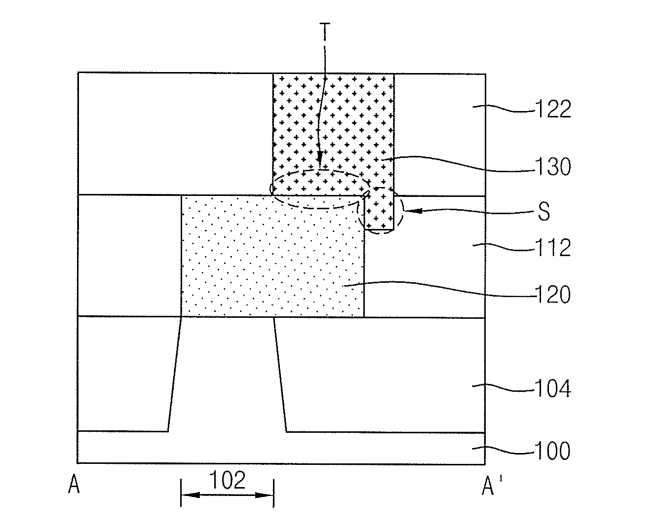
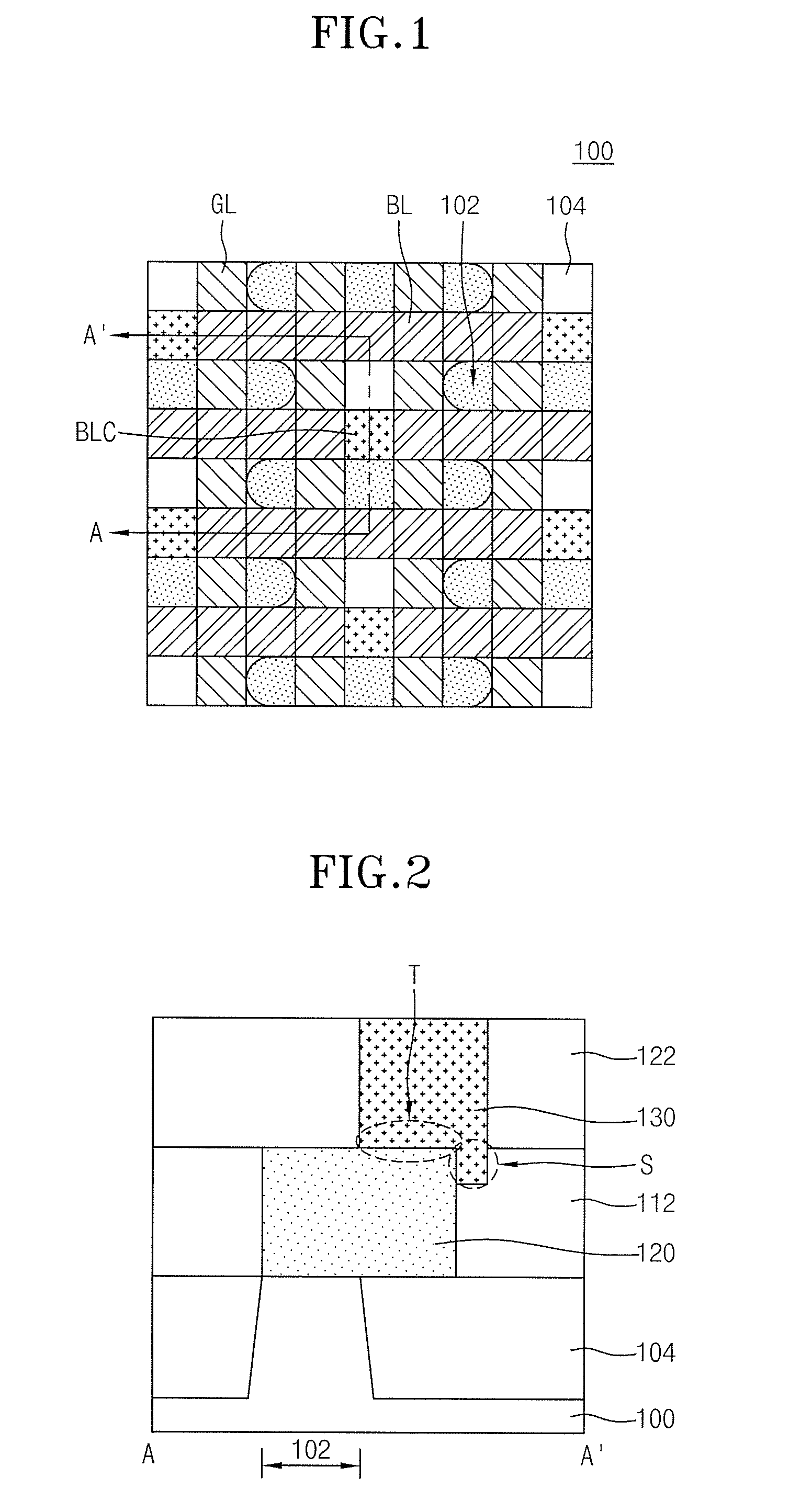
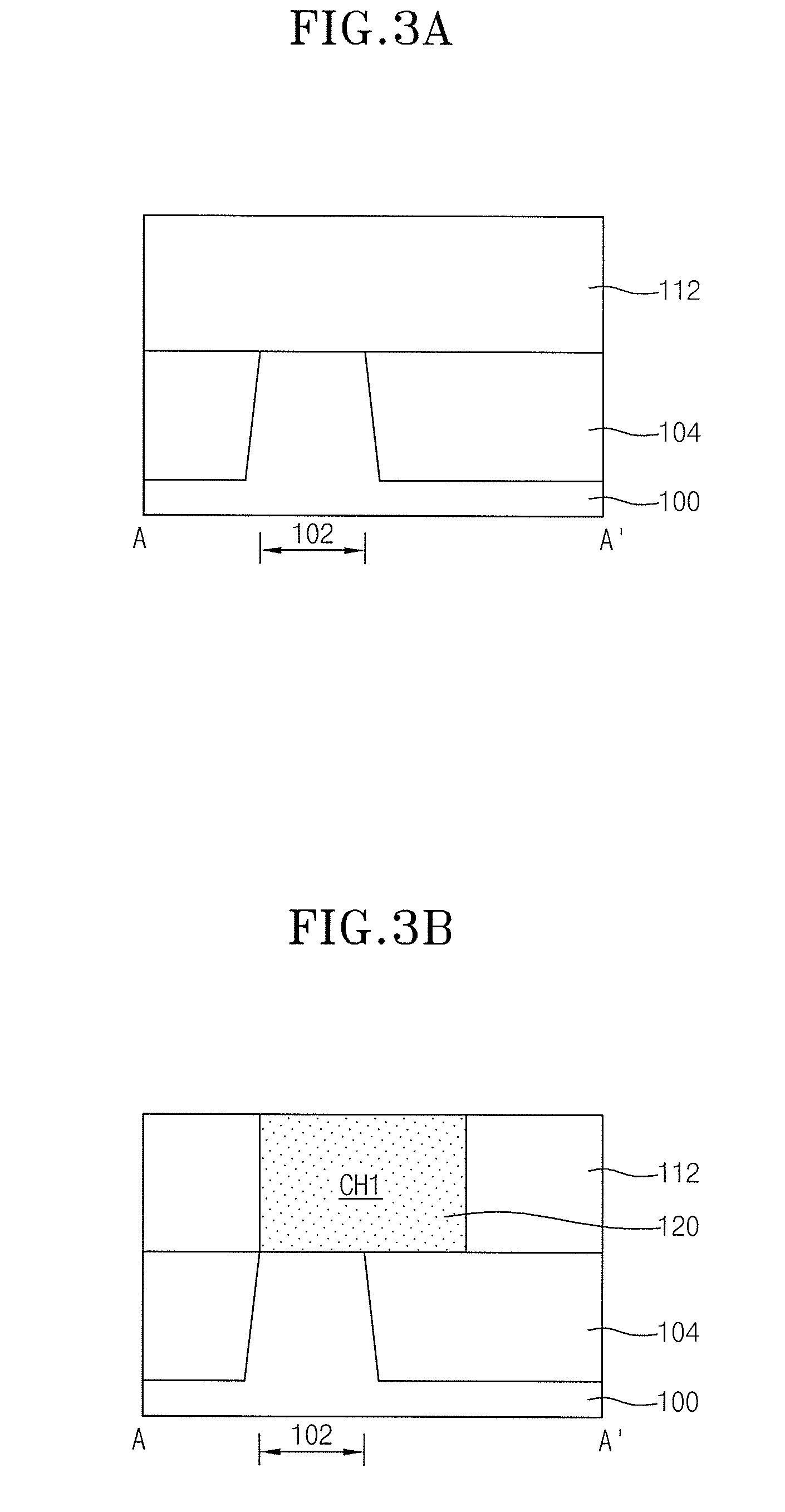
[0062]FIGS. 3A through 3E are cross-sectional views shown for illustrating the processes of a method for manufacturing the semiconductor device in accordance with the present invention.
[0063]Referring to FIG. 3A, an isolation structure 104 is formed in a semiconductor substrate 100 to delimit active regions. Subsequently, a plurality of gate lines (not shown) are formed on the active regions and the isolation structure 104. A first insulation layer 112 is formed on the semiconductor substrate 100 to fill the spaces between the gate lines. Preferably, the first insulation layer 112 is then planarized to expose the upper surfaces of the gate lines.
[0064]Referring to FIG. 3B, a portion of the planarized first insulation layer 112 is etched so as to define a first contact hole CH1 for a landing plug exposing a portion of the semiconductor substrate 100. Thereupon, a first plug 120, for example, a landing plug, is formed in the first contact hole CH1. The landing plug may comprise, for e...
second embodiment
[0083]In particular, in the present invention, since the portions S of the second plug 430, which contact the side surfaces of the upper part of the first plug 420, are formed of a material which has relatively low resistance, contact resistance can be effectively decreased.
[0084]While it was described and depicted in the above embodiment that the second plugs 430 comprise bit line contact plugs and the conductive patterns comprise bit lines BL, the present invention is not limited as such, for example, it is conceivable that the second plugs 430 can comprise storage node contact plugs and the conductive patterns can comprise storage nodes. Further, embodiments of the present invention can be applied to various types of contact plugs used in various types of semiconductor devices.
[0085]FIGS. 6A through 6G are cross-sectional views shown for illustrating the processes of a method for manufacturing the semiconductor device in accordance with the second embodiment of the present invent...
PUM
 Abstract
Description
Claims
Application Information
 - R&D
- Intellectual Property
- Life Sciences
- Materials
- Tech Scout
- Unparalleled Data Quality
- Higher Quality Content
- 60% Fewer Hallucinations
Browse by: Latest US Patents, China's latest patents, Technical Efficacy Thesaurus, Application Domain, Technology Topic, Popular Technical Reports.
© 2025 PatSnap. All rights reserved.Legal|Privacy policy|Modern Slavery Act Transparency Statement|Sitemap|About US| Contact US: help@patsnap.com


